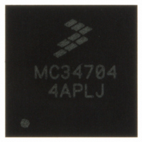
MC34704AEP Freescale Semiconductor, MC34704AEP Datasheet - Page 43

MC34704AEP
Manufacturer Part Number
MC34704AEP
Description
IC POWER MANAGEMENT 56-QFN
Manufacturer
Freescale Semiconductor
Datasheet
1.MC34704BEPR2.pdf
(54 pages)
Specifications of MC34704AEP
Applications
Processor
Current - Supply
86mA
Voltage - Supply
2.7 V ~ 5.5 V
Operating Temperature
-20°C ~ 85°C
Mounting Type
Surface Mount
Package / Case
56-QFN
Output Voltage
5 V
Input Voltage
2.7 V to 5.5 V
Switching Frequency
750 KHz to 2 MHz
Mounting Style
SMD/SMT
Number Of Outputs
8
Lead Free Status / RoHS Status
Lead free / RoHS Compliant
Compensating for boost operation:
• L: A boost power stage can be designed to operate in
stage is when the input voltage is equal to one half of the
output voltage, which results in the Maximum
• COUT: The three elements of output capacitor that
• R1 and RB:
desire value using a Vref=0.6V, select R1 between 10k and
100K and then calculate RB as follows:
Analog Integrated Circuit Device Data
Freescale Semiconductor
C
L
1. Define I
L
ESR
CCM for load currents above a certain level usually 5 to
15% of full load. The minimum value of inductor to
maintain CCM can be determined by using the following
procedure:
However the worst case condition for the boost power
contribute to its impedance and output voltage ripple are
the ESR, the ESL and the capacitance C. The minimum
capacitor value is approximately:
• Where
• Now calculate the maximum allowed ESR to reach the
These two resistors help to set the output voltage to the
min
OUT
min
15% of full load:
desired
≥
≥
≤
≥
Vo D
------------------------------------------ -
Vo T ( )
--------------- -
16I
-------------------------------------------- -
⎛
⎝
Io
---------------------------- -
FswΔVo
---------------------- -
1
max
( ) 1
Io
–
Δ
OB
OB
Δ
VO
D
max
2I
VO
(
D
ΔVo
max
as the minimum current to maintain CCM as
OB
max
r
–
r
is the desired output voltage ripple.
:
r
D
r
+
)
I
2
OB
T
⎞
⎠
Δ
[H]
[H]
[F]
I
L
, then:
[Ω]
• Compensation network. (C1,C2,C3, R2, R3)
frequencies referring to the plant are:
charge of canceling some of these poles and zeros to
achieve stability in the system. The following poles and
zeroes frequencies are provided by the type 3 compensation:
F
F
F
RB
1. Output LC filter cutoff frequency (F
D′
2. Cutoff frequency due to capacitor ESR:
3. The right plane zero frequency:
RHP
4. Crossover frequency (or bandwidth): select this
F
F
For compensating a boost converter, 4 important
• Where D’
The Type 3 external compensation network will be in
PO
P1
ESR
BW
LC
min
by:
frequency as far away form the RHP
possible:
=
=
=
«
Z
=
=
F
----------------------- -
------------- -
V
=
F
RHP
--------------- -
=
------------------------- -
2π
Vo
ESR
REF
--------------------------------------- -
2π C
BW
---------------------- -
Vout
6
R1
(
---------------------------------------- -
D′
Vin
D′
LC
(
Z
–
min
min
min
OUT
min
OUT
max
1
1
2πL
is the minimum off time percentage given
)
F
2
F
)ESR
R
Z1
2P
LOAD
=
=
FUNCTIONAL DEVICE OPERATION
0.9F
F
---------- -
SW
2
LC
COMPONENT CALCULATION
[Ω]
F
LC
22
Z
[Hz]
):
as much as
=
[Hz]
[Hz]
[Hz]
1.1F
LC
34704
43


