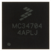
MC34704AEP Freescale Semiconductor, MC34704AEP Datasheet - Page 5

MC34704AEP
Manufacturer Part Number
MC34704AEP
Description
IC POWER MANAGEMENT 56-QFN
Manufacturer
Freescale Semiconductor
Datasheet
1.MC34704BEPR2.pdf
(54 pages)
Specifications of MC34704AEP
Applications
Processor
Current - Supply
86mA
Voltage - Supply
2.7 V ~ 5.5 V
Operating Temperature
-20°C ~ 85°C
Mounting Type
Surface Mount
Package / Case
56-QFN
Output Voltage
5 V
Input Voltage
2.7 V to 5.5 V
Switching Frequency
750 KHz to 2 MHz
Mounting Style
SMD/SMT
Number Of Outputs
8
Lead Free Status / RoHS Status
Lead free / RoHS Compliant
Table 2. 34704 Pin Definitions (continued)
Analog Integrated Circuit Device Data
Freescale Semiconductor
Pin Number Device Pin Name Pin Function
A functional description of each pin can be found in the Functional Pin Description section beginning on
23
11
12
13
14
15
16
17
18
19
20
21
22
24
25
26
27
28
29
(1)
A/B
A/B
A/B
A/B
A/B
A/B
A/B
A/B
A/B
A/B
A/B
A/B
A/B
A/B
A/B
A/B
A
B
A
B
A
B
COMP7
VOUT3
VOUT8
VOUT1
VREF7
PVIN3
FREQ
SW3
SW8
SW1
SDA
NC0
SCL
RST
NC1
NC2
FB3
FB8
BT8
BT1
VG
SS
Input/Output
Input/Output
No Connect
No Connect
No Connect
Open Drain
Passive
Passive
Passive
Passive
Output
Output
Output
Output
Output
Output
Output
Power
Input
Input
Input
Input
REG3 power supply input
voltage
REG3 switching node
REG3 output voltage
return pin
REG3 voltage feedback
input for voltage
regulation/programming
Soft start time
Oscillator frequency
REG8 voltage feedback
input for voltage
regulation/programming
REG8 bootstrap capacitor
input pin
REG8 regulated output
voltage pin
REG8 switching node
REG1 switching node
REG1 regulated output
voltage before the cutoff
switch
REG1 regulated output
voltage pin.
-
REG1 bootstrap capacitor
input pin
I
input
I
input
Power reset output signal
(Microprocessor Reset)
REG7 compensation
network connection
-
REG7 resistor feedback
network reference voltage
-
2
2
C serial interface clock
C serial interface data
Formal Name
This is the connection to the drain of the high side switch FET.
Input decoupling /filtering is required for proper REG3 operation.
Use a 10uf decoupling capacitor for better performance.
The inductor is connected between this pin and the regulated
REG3 output.
This is the discharge path of REG3 output voltage.
Connect the feedback resistor divider to this pin.
The soft start time for all regulators can be adjusted by
connecting this pin to an external resistor divider between VDDI
and AGND pins.
The oscillator frequency can be adjusted by connecting this pin
to an external resistor divider between VDDI and AGND pins.
This pin sets F
Connect the feedback resistor divider to this pin.
Connect a 0.01 μF capacitor between this pin and SW8 pin to
enhance the gate of the Synchronous Power MOSFET.
Connect this pin directly to the load directly and to the output
filter as close to the pin as possible.
The inductor is connected between this pin and the VIN pin.
The inductor is connected between this pin and the VIN Pin.
REG1 regulated output voltage before the cut-off switch. This
supplies the internal circuits and the gate drive
Connect this pin directly to the load directly and to the output
filter as close to the pin as possible.
Pin 23 is not connected.
Connect a 1.0 μF capacitor between this pin and SW1 pin to
enhance the gate of the Switch Power MOSFET.
I
I
This is an open drain output and must be pulled up by an
external resistor to a supply voltage like V
REG7 compensation network connection.
Pin 28 is not connected
Connect this pin to the bottom of the feedback resistor divider.
Pin 29 is not connected
2
2
C serial interface clock input.
C serial interface data input.
SW1
value.
Definition
page
PIN CONNECTIONS
IN
.
17.
34704
5


