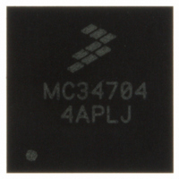
MC34704AEP Freescale Semiconductor, MC34704AEP Datasheet - Page 46

MC34704AEP
Manufacturer Part Number
MC34704AEP
Description
IC POWER MANAGEMENT 56-QFN
Manufacturer
Freescale Semiconductor
Datasheet
1.MC34704BEPR2.pdf
(54 pages)
Specifications of MC34704AEP
Applications
Processor
Current - Supply
86mA
Voltage - Supply
2.7 V ~ 5.5 V
Operating Temperature
-20°C ~ 85°C
Mounting Type
Surface Mount
Package / Case
56-QFN
Output Voltage
5 V
Input Voltage
2.7 V to 5.5 V
Switching Frequency
750 KHz to 2 MHz
Mounting Style
SMD/SMT
Number Of Outputs
8
Lead Free Status / RoHS Status
Lead free / RoHS Compliant
• L: The minimum value of inductor to maintain CCM can be
• C
C
• R1 and RB: These two resistors help to set the output
RB
VREF7 pin (VREF7=1.5 V) which provide a positive voltage
to assure a positive voltage at the FB7 pin.
• Compensation network. (C1,C2,C3, R2, R3)
frequencies referring to the plant are:
46
34704
FUNCTIONAL DEVICE OPERATION
COMPONENT CALCULATION
ESR
OUT
L
V
determined by using the following procedure:
contribute to its impedance and output voltage ripple are
the ESR, the ESL and the capacitance C. The minimum
capacitor value is approximately:
• Where
• Now calculate the maximum allowed ESR to reach the
voltage to the desire value using a
between 10 k and 150 K and then calculate RB as follows:
NOTE: RB is not grounded, instead is connected to
For compensating a buck converter, 4 important
min
RRM
OUT
=
desired.
≥
≥
------------------------------------ - R1
1.5
≤
: The three elements of output capacitor that
Io
---------------------------- -
------------------
2Io
≥
------------------------------------------------- -
⎛
⎝
F
–
-----------------------
1
max
SW
–
Vin
VoT
Io
–
max
0.9
Vo
Δ
Δ
D
max
D
VO
–
Vo
max
max
Δ
–
⎛
⎝
Vo
-------------------------------
Vo
Vo
r
0.9
r
is the desired output voltage ripple.
+
Vin
r
–
------------- -
1
Vin
I
OB
–
min
D
min
⎞
⎠
⎞
⎠
2
V
FB
7=0.6V, select R1
[H]
[F]
[Ω]
[Ω]
F
F
F
charge of canceling some of these poles and zeros to
achieve stability in the system. The following poles and
zeroes frequencies are provided by the type 3 compensation:
RHP
F
D′
F
PO
ESR
P1
LC
BW
min
• Output LC filter cutoff frequency (F
Where D’
• Cutoff frequency due to capacitor ESR:
• The right plane zero frequency:
• Crossover frequency (or bandwidth): select this
The Type 3 external compensation network will be in
=
=
=
Z
«
frequency as far away form the RHP
possible:
=
=
RHP
--------------- -
F
=
F
------------------------- -
2π
ESR
--------------------------------------- -
2π C
BW
------------------------- -
6
Vout
(
---------------------------------------- -
D′
LC
Vin
D′
(
min
Z
min
min
OUT
D 2πL
OUT
min
max
is the minimum off time percentage given by:
1
•
)
2
F
F
)ESR
R
Z1
2P
LOAD
=
Analog Integrated Circuit Device Data
=
0.9F
F
-----------
SW
2
LC
Freescale Semiconductor
F
22
LC
Z
=
):
as much as
1.1F
LC
[Hz]
[Hz]
[Hz]
[Hz]


