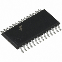
FAN5092MTC Fairchild Semiconductor, FAN5092MTC Datasheet - Page 16

FAN5092MTC
Manufacturer Part Number
FAN5092MTC
Description
IC CTRLR DC/DC SYNC BUCK 28TSSOP
Manufacturer
Fairchild Semiconductor
Type
Step-Down (Buck)r
Datasheet
1.FAN5092MTCX.pdf
(20 pages)
Specifications of FAN5092MTC
Internal Switch(s)
No
Synchronous Rectifier
No
Number Of Outputs
1
Voltage - Output
1.1 ~ 5 V
Frequency - Switching
200kHz ~ 2MHz
Voltage - Input
12V
Operating Temperature
0°C ~ 70°C
Mounting Type
Surface Mount
Package / Case
28-TSSOP
Output Voltage
17 V
Mounting Style
SMD/SMT
Operating Temperature Range
0 C to + 70 C
Lead Free Status / RoHS Status
Lead free / RoHS Compliant
Current - Output
-
Power - Output
-
Lead Free Status / Rohs Status
Lead free / RoHS Compliant
Other names
FAN5092MTC_NL
FAN5092MTC_NL
FAN5092MTC_NL
Available stocks
Company
Part Number
Manufacturer
Quantity
Price
Company:
Part Number:
FAN5092MTC
Manufacturer:
Fairchild Semiconductor
Quantity:
135
Part Number:
FAN5092MTCX
Manufacturer:
FAIRCHILD/仙童
Quantity:
20 000
FAN5092
For details and a spreadsheet on MOSFET selection, refer to
Applications Bulletin AB-8.
Gate Resistors
Use of a gate resistor on every MOSFET is mandatory. The
gate resistor prevents high-frequency oscillations caused by
the trace inductance ringing with the MOSFET gate
capacitance. The gate resistors should be located physically
as close to the MOSFET gate as possible.
The gate resistor also limits the power dissipation inside the
IC, which could otherwise be a limiting factor on the switch-
ing frequency. It may thus carry significant power, especially
at higher frequencies. As an example, consider the gate
resistors used for the low-side MOSFETs (Q2 and Q4) in
Figure 1. The FDB7045L has a maximum gate charge of
70nC at 5V, and an input capacitance of 5.4nF. The total
energy used in powering the gate during one cycle is the
energy needed to get it up to 5V, plus the energy to get it up
to 12V:
This power is dissipated every cycle, and is divided between
the internal resistance of the FAN5092 gate driver and the
gate resistor. Thus,
and each gate resistor thus requires a 1/4W resistor to ensure
worst case power dissipation.
The same calculation may be performed for the high-side
MOSFETs, bearing in mind that their gate voltage swings
only the charge pump voltage of 5V.
Inductor Selection
Choosing the value of the inductor is a tradeoff between
allowable ripple voltage and required transient response.
A smaller inductor produces greater ripple while producing
better transient response. In any case, the minimum induc-
tance is determined by the allowable ripple. The first order
equation (close approximation) for minimum inductance for
a two-slice converter is:
where:
Vin = Input Power Supply
Vout = Output Voltage
f = DC/DC converter switching frequency
16
P
E
Rgate
=
=
L
QV
482nJ
min
=
+
=
1
-- - C
2
------------------------------------------------ -
-------------------------------- -
4.7
R
V
---------------------------------- -
gate
E f R
in
4.7
–
V 2
+
+
2 V
1.0
f
R
=
internal
gate
70nC 5V
out
=
19mW
V
---------- -
V
out
in
=
+ 5.4nF
482nJ 300KHz
1
-- -
2
-----------------
V
ESR
ripple
12V 5V
–
2
ESR = Equivalent series resistance of all output capacitors in
parallel
Vripple = Maximum peak to peak output ripple voltage
budget.
One other limitation on the minimum size of the inductor is
caused by the current feedback loop stability criterion. The
inductor must be greater than:
where L is the inductance in Henries, R
resistance of one slice’s low-side MOSFET, R
value of the droop resistor in Ohms, V
and V
mula will not present any limitation on the selection of the
inductor value.
A typical value for the inductor is 1.3 H at an oscillator
frequency of 1.2MHz (300KHz each slice) and 220nH at an
oscillator frequency of 4MHz (1MHz each slice). For other
frequencies, use the interpolating formula
Schottky Diode Selection
The application circuit of Figure 1 shows a Schottky diode,
D1 (D2 respectively), one in each slice. They are used as
free-wheeling diodes to ensure that the body-diodes in the
low-side MOSFETs do not conduct when the upper
MOSFET is turning off and the lower MOSFETs are turning
on. It is undesirable for this diode to conduct because its high
forward voltage drop and long reverse recovery time
degrades efficiency, and so the Schottky provides a shunt
path for the current. Since this time duration is extremely
short, being minimized by the adaptive gate delay, the selec-
tion criterion for the diode is that the forward voltage of the
Schottky at the output current should be less than the forward
voltage of the MOSFET’s body diode. Power capability is
not a criterion for this device, as its dissipation is very small.
Output Filter Capacitors
The output bulk capacitors of a converter help determine its
output ripple voltage and its transient response. It has
already been seen in the section on selecting an inductor that
the ESR helps set the minimum inductance. For most con-
verters, the number of capacitors required is determined by
the transient response and the output ripple voltage, and
these are determined by the ESR and not the capacitance
value. That is, in order to achieve the necessary ESR to meet
the transient and ripple requirements, the capacitance value
required is already very large.
The most commonly used choice for output bulk capacitors
is aluminum electrolytics, because of their low cost and low
L 3 10
o
is the output voltage. For most applications, this for-
–
10
L nH
R
DS on
1.86 10
-------------------------- - 240
f KHz
R
Droop
PRODUCT SPECIFICATION
6
–
in
DS,on
is either 5V or 12V,
V
REV. 1.0.7 6/20/02
in
–
is the on-state
Droop
2V
o
is the


