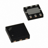
FAN2013MPX Fairchild Semiconductor, FAN2013MPX Datasheet - Page 3

FAN2013MPX
Manufacturer Part Number
FAN2013MPX
Description
IC CONV DC/DC 2A ADJ LV 6-MLP
Manufacturer
Fairchild Semiconductor
Type
Step-Down (Buck)r
Datasheet
1.FAN2013MPX.pdf
(9 pages)
Specifications of FAN2013MPX
Internal Switch(s)
Yes
Synchronous Rectifier
Yes
Number Of Outputs
1
Voltage - Output
0.8 ~ 4.5 V
Current - Output
2A
Frequency - Switching
1.3MHz
Voltage - Input
4.5 ~ 5.5 V
Operating Temperature
-40°C ~ 85°C
Mounting Type
Surface Mount
Package / Case
6-MLP
Lead Free Status / RoHS Status
Lead free / RoHS Compliant
Power - Output
-
Lead Free Status / Rohs Status
Lead free / RoHS Compliant
Other names
FAN2013MPXTR
Available stocks
Company
Part Number
Manufacturer
Quantity
Price
Part Number:
FAN2013MPX
Manufacturer:
FAIRCHILD/仙童
Quantity:
20 000
© 2006 Fairchild Semiconductor Corporation
FAN2013 Rev. 1.0.3
Absolute Maximum Ratings
Stresses exceeding the absolute maximum ratings may damage the device. The device may not function or be
operable above the recommended operating conditions and stressing the parts to these levels is not recommended.
In addition, extended exposure to stresses above the recommended operating conditions may affect device
reliability. The absolute maximum ratings are stress ratings only.
Notes:
1.
2.
Recommended Operating Conditions
The Recommended Operating Conditions table defines the conditions for actual device operation. Recommended
operating conditions are specified to ensure optimal performance to the datasheet specifications. Fairchild does not
recommend exceeding them or designing to Absolute Maximum Ratings.
Note:
3.
Symbols
Symbol
V
C
ESD
I
T
V
C
OUT
T
V
θ
Junction-to-ambient thermal resistance, θ
number of copper planes, number of via used, diameter of via used, available copper surface, and attached heat
sink characteristics.
Using Mil Std. 883E, method 3015.7 (Human Body Model) and EIA/JESD22C101-A (Charged Device Model).
Refer to the Applications section for details.
OUT
OUT
T
T
L
STG
JC
IN
IN
A
IN
L
J
Supply Voltage
Input Voltage on PVIN and Any Other Pin
Thermal Resistance, Junction-to-Tab
Lead Soldering Temperature (10 Seconds)
Storage Temperature
Junction Temperature
Supply Voltage Range
Output Voltage Range, Adjustable Version
Output Current
Inductor
Input Capacitor
Output Capacitor
Operating Ambient Temperature Range
Electrostatic Discharge Protection Level
(3)
(3)
(3)
Parameter
Parameter
JA
, is a strong function of PCB material, board thickness, thickness and
(1)
(2)
3
HBM
CDM
Min.
4.5
0.8
-40
10
20
Min.
Typ.
-0.3
-0.3
-65
-40
3.5
2.2
20
40
2
Max.
Max.
V
260
150
150
+85
6.2
V
5.5
2.0
IN
8
IN
-1
www.fairchildsemi.com
°C/W
Unit
Unit
kV
°C
°C
°C
µH
µF
µF
°C
V
V
V
V
A


