FSHDMI08MTDX Fairchild Semiconductor, FSHDMI08MTDX Datasheet - Page 4
FSHDMI08MTDX
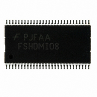
Manufacturer Part Number
FSHDMI08MTDX
Description
IC HDMI SWITCH DDC/CEC 56-TSSOP
Manufacturer
Fairchild Semiconductor
Datasheet
1.FSHDMI08MTDX.pdf
(11 pages)
Specifications of FSHDMI08MTDX
Applications
*
Mounting Type
Surface Mount
Package / Case
56-TSSOP
Lead Free Status / RoHS Status
Lead free / RoHS Compliant
Other names
FSHDMI08MTDXTR
Available stocks
Company
Part Number
Manufacturer
Quantity
Price
Company:

Part Number:
FSHDMI08MTDX
Manufacturer:
Fairchild Semiconductor
Quantity:
1 820
Part Number:
FSHDMI08MTDX
Manufacturer:
FAIRCHILD/仙童
Quantity:
20 000


© 2006 Fairchild Semiconductor Corporation
FSHDMI08 Rev. 1.0.4
Absolute Maximum Ratings
Stresses exceeding the absolute maximum ratings may damage the device. The device may not function or be
operable above the recommended operating conditions and stressing the parts to these levels is not recommended.
In addition, extended exposure to stresses above the recommended operating conditions may affect device
reliability. The absolute maximum ratings are stress ratings only.
Note:
1.
Recommended Operating Conditions
The Recommended Operating Conditions table defines the conditions for actual device operation. Recommended
operating conditions are specified to ensure optimal performance to the datasheet specifications. Fairchild does not
recommend exceeding them or designing to absolute maximum ratings.
V
V
V
V
Symbol
Symbol
V
V
V
SWTMDS
V
CNTRLT
CNTRLD
SWDDC
SWTMDS
V
V
ESD
V
T
V
CNTRLT
CNTRLD
SWDDC
I
The input and output negative ratings may be exceeded if the input and output diode current ratings are
observed.
θ
T
I
T
T
DDC
SW
STG
CC3
CC3
DDC
IK
JA
J
L
A
(1)
(1)
(1)
(1)
TMDS Supply Voltage – 3V
DDC Supply Voltage
Control Input Voltage – S
Control Input Voltage – S
Switch I/O Voltage for HDMI path
Switch I/O Voltage for DDC path
Operating Temperature
Thermal Resistance (Free Air)
Supply Voltage – TMDS Channels
Supply Voltage – 5V DDC
Switch I/O Voltage
Switch I/O Voltage
Control Input Voltage
Control Input Voltage
Input Clamp Diode Current
Switch I/O Current (Continuous)
Storage Temperature Range
Maximum Junction Temperature
Lead Temperature (Soldering, 10 Seconds)
Human Body Model (JEDEC: JESD22-A114)
Charged Device Model (JEDEC: JESD22-C101)
Parameter
1Dn+, 1Dn-, 2Dn+, 2Dn-, Dn+, Dn-, 1CLK+,
1CLK-, 2CLK+, 2CLK-, CLK+, CLK-
HPD1, HPD2, HPD, SCL1, SCL2, SCL,
SDA1, SDA2, SDA, CEC1, CEC2, CEC
S
S
TMDS
DDC
TMDS
DDC
Parameter
, /OE
, /OE
, /OE
, /OE
DDC
TMDS
DDC
TMDS
4
I/O to GND
All Other Pins
V
CC3
Min.
3.0
3.0
-40
0
0
0
– 0.6
Min.
-0.5
-0.5
-0.5
-0.5
-0.5
-0.5
-65
Max.
V
V
V
V
+85
+80
4.3
5.5
CC3
DDC
CC3
DDC
V
V
DDC
CC3
Max.
+150
+150
+260
128
-50
4.6
6.0
4.6
6.0
8.0
2.5
2.0
+ 0.3
+ 0.3
www.fairchildsemi.com
ºC/W
Unit
ºC
V
V
V
V
V
V
Unit
mA
mA
°C
°C
°C
kV
V
V
V
V
V
V
Related parts for FSHDMI08MTDX
Image
Part Number
Description
Manufacturer
Datasheet
Request
R

Part Number:
Description:
Fshdmi08 Low-voltage, Wide-bandwidth, Hdmi Switch With Ddc And Cec Multiplexer
Manufacturer:
Fairchild Semiconductor
Datasheet:
Part Number:
Description:
Fairchild Semiconductor [IGBT MODULE]
Manufacturer:
Fairchild Semiconductor
Datasheet:

Part Number:
Description:
Discrete Semiconductor Modules
Manufacturer:
Fairchild Semiconductor
Part Number:
Description:
Discrete Semiconductor Modules
Manufacturer:
Fairchild Semiconductor
Part Number:
Description:
This N-Channel MOSFET is produced using Fairchild Semiconductor’s advanced Power Trench® process
Manufacturer:
Fairchild Semiconductor
Datasheet:
Part Number:
Description:
This N-Channel MOSFET is produced using Fairchild Semiconductor’s advanced Power Trench® process
Manufacturer:
Fairchild Semiconductor
Datasheet:
Part Number:
Description:
This N-Channel MOSFET is produced using Fairchild Semiconductor’s advanced PowerTrench® process
Manufacturer:
Fairchild Semiconductor
Datasheet:
Part Number:
Description:
This N-Channel MOSFET is produced using Fairchild Semiconductor’s advanced PowerTrench® process
Manufacturer:
Fairchild Semiconductor
Datasheet:
Part Number:
Description:
This N-Channel MOSFET is produced using Fairchild Semiconductor’s advanced Power Trench® process
Manufacturer:
Fairchild Semiconductor
Datasheet:
Part Number:
Description:
This N-Channel logic Level MOSFETs are produced using Fairchild Semiconductor‘s advanced Power Trench® process that has been special tailored to minimize the on-state resistance and yet maintain superior switching performance
Manufacturer:
Fairchild Semiconductor
Datasheet:
Part Number:
Description:
This N-Channel MOSFET is produced using Fairchild Semiconductor’s advanced Power Trench® process
Manufacturer:
Fairchild Semiconductor
Datasheet:
Part Number:
Description:
This N-Channel SyncFET™ is produced using Fairchild Semiconductor’s advanced PowerTrench® process
Manufacturer:
Fairchild Semiconductor
Datasheet:
Part Number:
Description:
This N-Channel SyncFET™ is produced using Fairchild Semiconductor’s advanced PowerTrench® process
Manufacturer:
Fairchild Semiconductor
Datasheet:
Part Number:
Description:
This N-Channel SyncFET™ is produced using Fairchild Semiconductor’s advanced PowerTrench® process
Manufacturer:
Fairchild Semiconductor
Datasheet:
Part Number:
Description:
This N-Channel logic Level MOSFETs are produced using Fairchild Semiconductor‘s advanced Power Trench® process that has been special tailored to minimize the on-state resistance and yet maintain superior switching performance
Manufacturer:
Fairchild Semiconductor
Datasheet: