MT9HTF6472RHY-667D1 Micron Technology Inc, MT9HTF6472RHY-667D1 Datasheet
MT9HTF6472RHY-667D1
Specifications of MT9HTF6472RHY-667D1
Available stocks


Related parts for MT9HTF6472RHY-667D1


MT9HTF6472RHY-667D1 Summary of contents
Page 1
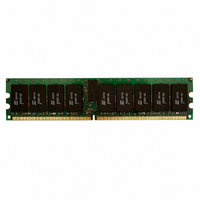
DDR2 SDRAM SORDIMM MT9HTF6472RH – 512MB MT9HTF12872RH – 1GB Features • 200-pin, small-outline registered dual in-line memo- ry module • Fast data transfer rates: PC2-4200, PC2-5300, or PC2-6400 • 512MB (64 Meg x 72) or 1GB (128 Meg x 72) ...
Page 2
... Table 3: Part Numbers and Timing Parameters – 512MB Modules 1 Base device: MT47H64M8, 512Mb DDR2 SDRAM Module 2 Part Number Density MT9HTF6472RH(I)Y-80E__ MT9HTF6472RH(I)Y-800__ MT9HTF6472RH(I)Y-667__ MT9HTF6472RH(I)Y-53E__ Table 4: Part Numbers and Timing Parameters – 1GB Modules 1 Base device: MT47H128M8, 1Gb DDR2 SDRAM Module 2 Part Number Density MT9HTF12872RH(I)Y-80E__ MT9HTF12872RH(I)Y-800__ MT9HTF12872RH(I)Y-667__ MT9HTF12872RH(I)Y-53E__ 1. The data sheet for the base device can be found on Micron’ ...
Page 3
Pin Assignments Table 5: Pin Assignments 200-Pin SORDIMM Front Pin Symbol Pin Symbol Pin DQ18 101 REF 3 DQ0 53 DQ19 103 105 DQ1 57 DQ24 107 9 DQS0# 59 ...
Page 4
... Pin Descriptions The pin description table below is a comprehensive list of all possible pins for all DDR2 modules. All pins listed may not be supported on this module. See Pin Assignments for information specific to this module. Table 6: Pin Descriptions Symbol Type Ax Input BAx Input ...
Page 5
Table 6: Pin Descriptions (Continued) Symbol Type SDA I/O RDQSx, Output RDQS#x Err_Out# Output (open drain Supply DD DDQ V Supply DDSPD V Supply REF V Supply SS – NC – NF – NU – RFU PDF: 09005aef828742dd ...
Page 6
Functional Block Diagram Figure 2: Functional Block Diagram RS0# DQS0# DQS0 DM0 DM CS# DQS DQS# DQ0 DQ DQ DQ1 DQ DQ2 DQ DQ3 DQ DQ4 DQ DQ5 DQ DQ6 DQ DQ7 DQS1# DQS1 DM1 DM CS# DQS DQS# DQ ...
Page 7
... DRAM core and eight corresponding n-bit-wide, one-half-clock-cycle data trans- fers at the I/O pins. DDR2 modules use two sets of differential signals: DQS, DQS# to capture data and CK and CK# to capture commands, addresses, and control signals. Differential clocks and data strobes ensure exceptional noise immunity for these signals and provide precise crossing points to capture input signals ...
Page 8
Electrical Specifications Stresses greater than those listed may cause permanent damage to the module. This is a stress rating only, and functional operation of the module at these or any other condi- tions outside those indicated in the device data ...
Page 9
... Design Considerations Simulations Micron memory modules are designed to optimize signal integrity through carefully de- signed terminations, controlled board impedances, routing topologies, trace length matching, and decoupling. However, good signal integrity starts at the system level. Mi- cron encourages designers to simulate the signal characteristics of the system's memo- ry bus to ensure adequate signal integrity of the entire memory system ...
Page 10
I Specifications DD Table 9: DDR2 I Specifications and Conditions – 512MB DD Values shown for MT47H64M8 DDR2 SDRAM only and are computed from values specified in the 512Mb (64 Meg x 8) component data sheet Parameter Operating one bank ...
Page 11
Table 9: DDR2 I Specifications and Conditions – 512MB (Continued) DD Values shown for MT47H64M8 DDR2 SDRAM only and are computed from values specified in the 512Mb (64 Meg x 8) component data sheet Parameter Operating bank interleave read current: ...
Page 12
Table 10: DDR2 I Specifications and Conditions – 1GB DD Values shown for MT47H128M8 DDR2 SDRAM only and are computed from values specified in the 1Gb (128 Meg x 8) com- ponent data sheet Parameter Operating one bank active-precharge current: ...
Page 13
Register and PLL Specifications Table 11: Register Specifications SSTU32872 devices or equivalent Parameter Symbol DC high-level V Control, command, IH(DC) input voltage DC low-level V Control, command, IL(DC) input voltage AC high-level V Control, command, IH(AC) input voltage AC low-level ...
Page 14
Table 12: PLL Specifications CUA845 device or JEDEC82-21 equivalent Parameter Symbol DC high-level V IH input voltage DC low-level V IL input voltage Input voltage (limits Input differential-pair V IX cross voltage Input differential volt- V ID(DC) age ...
Page 15
Temperature Sensor with Serial Presence-Detect EEPROM The temperature sensor continuously monitors the module’s temperature and can be read back at any time over the I Table 14: Temperature Sensor with Serial Presence-Detect EEPROM Operating Conditions Parameter/Condition Supply voltage Supply current: ...
Page 16
The interrupt mode enables software to reset EVENT# after a critical temperature thresh- old has been detected. Threshold points are set in the configuration register by the user. This mode triggers the critical temperature limit and both the MIN and ...
Page 17
Figure 3: EVENT# Pin Functionality Critical Alarm window (MAX) Alarm window (MIN) EVENT# interrupt mode EVENT# comparator mode EVENT# critical temperature only mode Table 16: Temperature Sensor Registers Name Pointer register Capability register Configuration register Alarm temperature upper boundary register ...
Page 18
Table 17: Pointer Register Bits 0– Table 18: Pointer Register Bits 0–2 Descriptions Capability Register The capability register indicates the features and functionality supported by the temper- ature sensor. ...
Page 19
Table 20: Capability Register Bit Description (Continued) Bit Description 4:3 Temperature resolution 00: 0.5°C LSB 01: 0.25°C LSB 10: 0.125°C LSB 11: 0.0625°C LSB 15:5 0: Must be set to zero Configuration Register Table 21: Configuration Register (Address: 0x01) 15 ...
Page 20
Table 22: Configuration Register Bit Descriptions (Continued) Bit Description 6 Alarm window lock bit 0: Alarm trips are not locked and can be changed 1: Alarm trips are locked and cannot be changed 7 Critical trip lock bit 0: Critical ...
Page 21
Figure 4: Hysteresis Applied to Temperature Around Trip Points Below window bit Above window bit 1. T Notes Hyst is the value set in the hysteresis bits of the configuration register. Table 23: Hysteresis Applied to Alarm ...
Page 22
Temperature Trip Point Registers The upper and lower temperature boundary registers are used to set the maximum and minimum values of the alarm window. LSB for these registers is 0.25°C. All RFU bits in the register will always report zero. ...
Page 23
Table 27: Temperature Register (Address: 0x05 Above Above Below MSB critical alarm alarm trip window window Table 28: Temperature Register Bit Descriptions Bit Description 13 Below alarm window 0: Temperature is equal to or above the lower ...
Page 24
Module Dimensions Figure 5: 200-Pin DDR2 SORDIMM 2.0 (0.079) R (2X) U1 1.0 (0.039) R (2X) 1.8 (0.071) (2X) 6.0 (0.236) TYP 2.0 (0.079) TYP U10 3.50 (0.138) TYP Pin 200 1.0 (0.039) TYP 1. All dimensions are in millimeters ...