MT9HTF6472RHY-667D1 Micron Technology Inc, MT9HTF6472RHY-667D1 Datasheet - Page 7
MT9HTF6472RHY-667D1
Manufacturer Part Number
MT9HTF6472RHY-667D1
Description
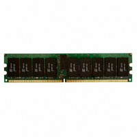
MODULE DDR2 512MB 200-SORDIMM
Manufacturer
Micron Technology Inc
Datasheet
1.MT9HTF6472RHY-667D1.pdf
(24 pages)
Specifications of MT9HTF6472RHY-667D1
Memory Type
DDR2 SDRAM
Memory Size
512MB
Speed
667MT/s
Package / Case
200-SORDIMM
Lead Free Status / RoHS Status
Lead free / RoHS Compliant
Available stocks
Company
Part Number
Manufacturer
Quantity
Price
Company:

Part Number:
MT9HTF6472RHY-667D1
Manufacturer:
FREESCALE
Quantity:
9 240


General Description
Serial Presence-Detect EEPROM Operation
Register and PLL Operation
Temperature Sensor
PDF: 09005aef828742dd
htf9c64_128x72rh.pdf - Rev. D 3/10 EN
DDR2 SDRAM modules are high-speed, CMOS dynamic random access memory mod-
ules that use internally configured 4 or 8-bank DDR2 SDRAM devices. DDR2 SDRAM
modules use DDR architecture to achieve high-speed operation. DDR2 architecture is
essentially a 4n-prefetch architecture with an interface designed to transfer two data
words per clock cycle at the I/O pins. A single read or write access for the DDR2 SDRAM
module effectively consists of a single 4n-bit-wide, one-clock-cycle data transfer at the
internal DRAM core and eight corresponding n-bit-wide, one-half-clock-cycle data trans-
fers at the I/O pins.
DDR2 modules use two sets of differential signals: DQS, DQS# to capture data and CK
and CK# to capture commands, addresses, and control signals. Differential clocks and
data strobes ensure exceptional noise immunity for these signals and provide precise
crossing points to capture input signals. A bidirectional data strobe (DQS, DQS#) is trans-
mitted externally, along with data, for use in data capture at the receiver. DQS is a
strobe transmitted by the DDR2 SDRAM device during READs and by the memory con-
troller during WRITEs. DQS is edge-aligned with data for READs and center-aligned
with data for WRITEs.
DDR2 SDRAM modules operate from a differential clock (CK and CK#); the crossing of
CK going HIGH and CK# going LOW will be referred to as the positive edge of CK. Com-
mands (address and control signals) are registered at every positive edge of CK. Input
data is registered on both edges of DQS, and output data is referenced to both edges of
DQS, as well as to both edges of CK.
DDR2 SDRAM modules incorporate serial presence-detect. The SPD data is stored in a
256-byte EEPROM. The first 128 bytes are programmed by Micron to identify the mod-
ule type and various SDRAM organizations and timing parameters. The remaining 128
bytes of storage are available for use by the customer. System READ/WRITE operations
between the master (system logic) and the slave EEPROM device occur via a standard
I
(WP) is connected to V
DDR2 SDRAM modules operate in registered mode, where the command/address input
signals are latched in the registers on the rising clock edge and sent to the DDR2
SDRAM devices on the following rising clock edge (data access is delayed by one clock
cycle). A phase-lock loop (PLL) on the module receives and redrives the differential
clock signals (CK, CK#) to the DDR2 SDRAM devices. The registers and PLL minimize
system and clock loading. PLL clock timing is defined by JEDEC specifications and en-
sured by use of the JEDEC clock reference board. Registered mode will add one clock
cycle to CL.
An on-board temperature sensor provides the ability to monitor the module tempera-
ture along with monitoring alarms. Programmable registers can be used to specify
temperature events and critical boundaries. An EVENT# pin is used to signal when dif-
ferent conditions occur based on how the registers are defined.
2
C bus using the DIMM’s SCL (clock) SDA (data), and SA (address) pins. Write protect
512MB, 1GB (x72, ECC, SR) 200-Pin DDR2 SDRAM SORDIMM
SS
, permanently disabling hardware write protection.
7
Micron Technology, Inc. reserves the right to change products or specifications without notice.
General Description
© 2007 Micron Technology, Inc. All rights reserved.
Related parts for MT9HTF6472RHY-667D1
Image
Part Number
Description
Manufacturer
Datasheet
Request
R

Part Number:
Description:
IC SDRAM 64MBIT 133MHZ 54TSOP
Manufacturer:
Micron Technology Inc
Datasheet:

Part Number:
Description:
IC SDRAM 64MBIT 5.5NS 86TSOP
Manufacturer:
Micron Technology Inc
Datasheet:
Part Number:
Description:
IC SDRAM 64MBIT 200MHZ 86TSOP
Manufacturer:
Micron Technology Inc
Datasheet:
Part Number:
Description:
IC SDRAM 64MBIT 133MHZ 54TSOP
Manufacturer:
Micron Technology Inc
Datasheet:
Part Number:
Description:
IC SDRAM 128MBIT 133MHZ 54TSOP
Manufacturer:
Micron Technology Inc
Datasheet:

Part Number:
Description:
IC SDRAM 256MBIT 133MHZ 90VFBGA
Manufacturer:
Micron Technology Inc
Datasheet:
Part Number:
Description:
IC SDRAM 128MBIT 133MHZ 54TSOP
Manufacturer:
Micron Technology Inc
Datasheet:
Part Number:
Description:
IC SDRAM 256MBIT 133MHZ 54TSOP
Manufacturer:
Micron Technology Inc
Datasheet:

Part Number:
Description:
IC DDR SDRAM 512MBIT 6NS 66TSOP
Manufacturer:
Micron Technology Inc
Datasheet:
Part Number:
Description:
IC SDRAM 128MBIT 167MHZ 86TSOP
Manufacturer:
Micron Technology Inc
Datasheet:
Part Number:
Description:
IC SDRAM 128MBIT 143MHZ 86TSOP
Manufacturer:
Micron Technology Inc
Datasheet:

Part Number:
Description:
SDRAM 256M-BIT 1.8V 54-PIN VFBGA
Manufacturer:
Micron Technology Inc
Datasheet:
Part Number:
Description:
IC SDRAM 128MBIT 143MHZ 86TSOP
Manufacturer:
Micron Technology Inc
Datasheet:

Part Number:
Description:
IC SDRAM 128MBIT 125MHZ 54VFBGA
Manufacturer:
Micron Technology Inc
Datasheet:
Part Number:
Description:
IC SDRAM 128MBIT 125MHZ 54VFBGA
Manufacturer:
Micron Technology Inc
Datasheet: