AC162078 Microchip Technology, AC162078 Datasheet - Page 77
AC162078
Manufacturer Part Number
AC162078
Description
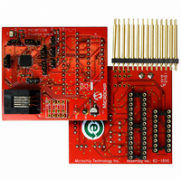
HEADER INTRFC MPLAB ICD2 18F1330
Manufacturer
Microchip Technology
Datasheet
1.AC162078.pdf
(318 pages)
Specifications of AC162078
Accessory Type
Transition Header
Lead Free Status / RoHS Status
Not applicable / Not applicable
For Use With/related Products
ICD2
Lead Free Status / RoHS Status
Lead free / RoHS Compliant, Not applicable / Not applicable
Available stocks
Company
Part Number
Manufacturer
Quantity
Price
Company:

Part Number:
AC162078
Manufacturer:
MICROCHIP
Quantity:
12 000


7.5
The minimum programming block is 4 words or 8 bytes.
Word or byte programming is not supported.
Table writes are used internally to load the holding
registers needed to program the Flash memory. There
are 8 holding registers used by the table writes for
programming.
Since the Table Latch (TABLAT) is only a single byte,
the TBLWT instruction may need to be executed 8 times
for each programming operation. All of the table write
operations will essentially be short writes because only
the holding registers are written. At the end of updating
the 8 holding registers, the EECON1 register must be
written to in order to start the programming operation with
a long write.
FIGURE 7-5:
7.5.1
The sequence of events for programming an internal
program memory location should be:
1.
2.
3.
4.
5.
6.
7.
2009 Microchip Technology Inc.
TBLPTR = xxxxx0
Read 8 bytes into RAM.
Update data values in RAM as necessary.
Load Table Pointer register with address being
erased.
Execute the row erase procedure.
Load Table Pointer register with address of first
byte being written.
Write the 8 bytes into the holding registers with
auto-increment.
Set the EECON1 register for the write operation:
• set EEPGD bit to point to program memory;
• clear the CFGS bit to access program memory;
• set WREN to enable byte writes.
Writing to Flash Program Memory
FLASH PROGRAM MEMORY
WRITE SEQUENCE
Holding Register
TABLE WRITES TO FLASH PROGRAM MEMORY
8
TBLPTR = xxxxx1
Holding Register
8
Program Memory
TBLPTR = xxxxx2
Write Register
TABLAT
The long write is necessary for programming the
internal Flash. Instruction execution is halted while in a
long write cycle. The long write will be terminated by
the internal programming timer.
The EEPROM on-chip timer controls the write time.
The write/erase voltages are generated by an on-chip
charge pump, rated to operate over the voltage range
of the device.
8.
9.
10. Write 0AAh to EECON2.
11. Set the WR bit. This will begin the write cycle.
12. The CPU will stall for duration of the write (about
13. Re-enable interrupts.
14. Verify the memory (table read).
This procedure will require about 6 ms to update one
row of 8 bytes of memory. An example of the required
code is given in Example 7-3.
Note:
Note:
Holding Register
Disable interrupts.
Write 55h to EECON2.
2 ms using internal timer).
PIC18F1230/1330
The default value of the holding registers on
device Resets and after write operations is
FFh. A write of FFh to a holding register
does not modify that byte. This means that
individual bytes of program memory may be
modified, provided that the change does not
attempt to change any bit from a ‘0’ to a ‘1’.
When modifying individual bytes, it is not
necessary to load all 8 holding registers
before executing a write operation.
Before setting the WR bit, the Table
Pointer address needs to be within the
intended address range of the 8 bytes in
the holding register.
8
TBLPTR = xxxxx7
Holding Register
DS39758D-page 77
8
Related parts for AC162078
Image
Part Number
Description
Manufacturer
Datasheet
Request
R

Part Number:
Description:
Manufacturer:
Microchip Technology Inc.
Datasheet:
Part Number:
Description:
Manufacturer:
Microchip Technology Inc.
Datasheet:
Part Number:
Description:
Manufacturer:
Microchip Technology Inc.
Datasheet:
Part Number:
Description:
Manufacturer:
Microchip Technology Inc.
Datasheet:
Part Number:
Description:
Manufacturer:
Microchip Technology Inc.
Datasheet:
Part Number:
Description:
Manufacturer:
Microchip Technology Inc.
Datasheet:
Part Number:
Description:
Manufacturer:
Microchip Technology Inc.
Datasheet:
Part Number:
Description:
Manufacturer:
Microchip Technology Inc.
Datasheet: