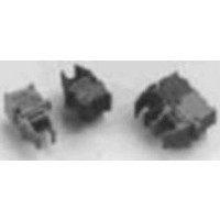
HFBR-0528 Avago Technologies US Inc., HFBR-0528 Datasheet - Page 9

HFBR-0528
Manufacturer Part Number
HFBR-0528
Description
KIT EVAL FIBER OPTIC 10MBD
Manufacturer
Avago Technologies US Inc.
Datasheet
1.HFBR-0528.pdf
(16 pages)
Specifications of HFBR-0528
Main Purpose
Interface, Fiber Optics
Embedded
No
Utilized Ic / Part
HFBR-1528, HFBR-2528
Primary Attributes
10MBd, Communication up to 50m using 1mm POF
Secondary Attributes
Crimpless Connectors
Silicon Core Number
HFBR-1528, HFBR-2528
Kit Contents
TX/RX Mods, Cable, Pol Kit, SW, Pwr. Sup
Silicon Family Name
Versatile Link
Features
Fiber Optic Transmitter And Receiver
Lead Free Status / RoHS Status
Lead free / RoHS Compliant
Other names
516-2144
HFBR-0528
HFBR-0528
TTL
CMOS
INPUT
2. Transmitter Drive Circuits
LED-based transmitters are easy and simple to drive
because the current through the LED is proportional to
the optical output power. The current can be amplitude
modulated using only a switching transistor and a single
resistor in series with the LED. Because of the simplicity
of the drive circuit, the design engineer has many op-
tions to realize this function. As mentioned previously,
the HFBR-0508Z link performance is guaranteed when
using the drive circuit in the data sheet (see also 2.2), as
it meets most application requirements. The pros and
cons of a few other approaches that will help design en-
gineers to optimize their link performance for specific
applications are discussed in the following section.
2.1. Pros and Cons of Parallel and Series Transmitter Drive
Circuits
Basically, two methods exist for driving LEDs. One uses
a series driver (Figure 9), the other is based on a parallel
driving scheme (Figure 4). Series driving circuits con-
sume only half the power but generate higher transient
noise in the power supply line when the LED current is
switching. The parallel driver uses a constant current
from the power supply rail, thus minimizing power sup-
ply noise, which could couple into the receiver and de-
grade sensitivity. The parallel drive circuit also presents a
very low impedance to the LED junction during turn off.
This low impedance rapidly discharges the junction and
quickly extinguishes the optical output of the LED.
One should keep in mind that the transmitter drive cir-
cuit topology contributes to the overall pulse-width
distortion (PWD) of the fiber optic link. Therefore, it is
important that the optical rise and fall times are fast com-
pared to the symbol time. The transmitter propagation
delay times, t
for the PWD of the entire link to be low. Fortunately,
the HFBR-528Z transmitter has rise and fall times that
are fast enough to be switched without peaking and
prebias
the drive circuit as simple as possible. Drive circuits for
rise and fall times on the order of 3 ns are discussed in
AN066
9
Figure 14. PNP Shunt Drive Circuit.
V cc
5510-14
[3]
[3]
for data rates as high as 0 MBd. This keeps
.
PLH
1 µF
and t
PHL
, should also be equally balanced
0.1
µF
R
2, 3, 4
1
16
14
12
10
8
6
4
2
0.1 0.2
HFBR-1528Z
PIN 5 & 8 SHOULD
BE CONNECTED
TO GROUND
RISE TIME
PARALLEL RESISTOR Rp (OHM) THOUSANDS
I
F
8
5
= 60 mA, T
2.2. Series Driver Circuit using Standard TTL Buffer ICs
Data sheet Drive Circuit
The driver circuit, Figure 9, is designed in such a way that
the LED is in series with the open-collector output of the
driving gate. Resistor R2 sets the drive current through
the LED, and resistor R provides a discharge path when
IL(dB) = 20
the LED forward current is turned off.
Equation III/2:
The low-impedance path R quickly discharges the LED,
decreasing the optical fall time. A 2 kOhm resistor was
empirically found to be an optimum value for best PWD.
It is important to note that capacitors C and C2 near the
LED anode filter the noise in the power supply line dur-
ing switching periods.
Figure 6 shows how LED forward current deviates from
the intended or nominal room temperature design val-
ue when using a series drive circuit, due to the following
factors:
a. part-to-part variations in LED forward voltage,
b. current-limiting resistor tolerance,
c. power supply tolerance, and
d. variations in the Vce saturation potential of the 7545
Figure 15: Typical Optical Switching Speed vs. Parallel Resistor R1.
l(max) =
P (T) = P (25) –
P (dBm) = 10
0.5
l(min) =
l =
V (T) = V (25)
R1 =
T
16
14
12
10
F
8
6
4
2
peripheral driver.
0.1 0.2
P (min)
RISE TIME
T
vp =
PARALLEL RESISTOR Rp (OHM) THOUSANDS
I
F
1
A
= 60 mA, T
Vcc - Vce - V
PWD
= 25 C, 1 m HCS
0.5
T
•
Pt(max) - P
−
P (min) - P
I
F
log
•
F
T
c
n
2
1
A
P
PWD
log
= 25 C, 1 m HCS
in m/s
RL, min
a(min)
2
a(max)
−
d2
d1
F
P(mW)
5
1mW
+ 20
5
−
∆
∆
a(max)
RL, max
∆
∆
RL, min
10
P
V
IL(max)
T
T
T
F
•
•
FALL TIME
20
log
10
• (T – 25)
(T – 25)
(in m)
- IL - OPM
−
50 100
OPM
NA2
FALL TIME
20
NA1
48.5
48.0
47.5
47.0
46.5
46.0
45.5
45.0
(m)
50 100
48.5
48.0
47.5
47.0
46.5
46.0
45.5
45.0


