QF1DA512-DK Quickfilter Technologies LLC, QF1DA512-DK Datasheet
QF1DA512-DK
Specifications of QF1DA512-DK


Related parts for QF1DA512-DK


QF1DA512-DK Summary of contents
Page 1
... QF1Da512-QN-T 16-Pin QFN - Tape & Reel (Reel qty 1000) QF1Da512-QN-B - Trays (tray qty 496) QF1D512-DK Base 1D Development Kit QF1Da512-DK 1Da Audio Dragon Platform Characteristic data and other specifications are subject to change without notice. Simple and versatile FIR engine (SavFIRe dSCK dSDI ...
Page 2
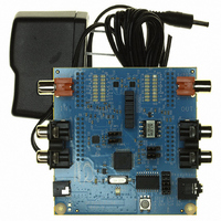
... QUICKFILTER DEVELOPMENT ENVIRONMENT QF1Da512-DK Audio Evaluation Platform Daughter card with stereo RCA jacks for input and output Also support SPDIF inputs and outputs QF1D512-DK; Motherboard Host for configuring and programming QF1Da512-DK via USB QF1Da512 PRELIMINARY DATA SHEET 2 QF1Da512 ...
Page 3
... Data Format and Control ............................................................................................................................... 10 Averaging and Down-sampler ...................................................................................................................... 10 Finite Impulse Response Filter (FIR) ............................................................................................................ 10 Digital Gain and Compression (DGC) .......................................................................................................... 10 Configuration Interface ................................................................................................................................. 10 4 SOFTWARE .............................................................................................................................................. 11 Device Configuration..................................................................................................................................... 11 Quickfilter Audio Development Kit (QF1Da512-DK) .................................................................................... 11 Quickfilter Host Development Kit (QF1D512-DK) ........................................................................................ 11 5 GENERAL OPERATION ........................................................................................................................... 11 6 CONFIGURATION INTERFACE ............................................................................................................... 12 SPI, Serial Peripheral Bus ............................................................................................................................. 12 6.1.1 ...
Page 4
... Normal SPI Mode ................................................................................................................................ 32 12.4 Continuous SPI Mode (CS_N tied to GND) ........................................................................................ 32 12.5 Synchronous Serial Mode (uP clock slave) ...................................................................................... 33 12.6 Inline SPI DAC ..................................................................................................................................... 33 ADC Configuration Read / Write – QF1Da512 Passthrough ............................................................ 34 12.7 12.8 QF1Da512 Configuration Mode .......................................................................................................... 34 13 I2C OPTION .............................................................................................................................................. 35 13.1 Mode of Operation .............................................................................................................................. 35 13.2 Data Format ......................................................................................................................................... 37 14 DGC USER GUIDANCE ...
Page 5
... Failure to observe proper handling and installation procedures can cause damage. Package Assembly The QF1Da512 is offered in a “green” package (RoHS & no Sb/Br), assembled with enhanced environmentally compatible Pb-free and halide-free materials. The leads possess a matte-tin plating which is compatible with conventional board assembly processes or newer lead-free board assembly processes. The peak soldering temperature should not exceed 260° ...
Page 6
... 500 kHz, 512 taps S - Standby - kHz 299 kHz 500 kHz S - Standby = 3.6V DD33 = 3.0V DD33 = 3.0V -100uA DD33 OH = 3.0V 100uA DD33 OL 6 QF1Da512 Min Typ Max Units Note 1.3 mA 6 200 uA 400 2.0 5.5 V -0.3 0.8 V +/- 1 ...
Page 7
... SDO high-Z time Rev A8 January 7, 2009 PRELIMINARY DATA SHEET Timing tcss tclh tcll tdis tdih tdov2 Parameters Parameter (SPI Input) * Using default cSCK capture/drive polarity. 7 tcsh tcs tdoz hi-z Min Max Units Note 500 KHz 20 MHz www.quickfiltertech.com QF1Da512 ...
Page 8
... NOTE: For tdov1 and tdov2, the output pin is set with I Rev A8 January 7, 2009 PRELIMINARY DATA SHEET Data Path Timing (all modes) tdlh tdll tdih tdov2 Parameters Parameter(SPI Output) 8 tdsh tds tdoz Min Max Units Note 500 KHz 24 MHz 4mA and C at 7pf. load load www.quickfiltertech.com QF1Da512 ...
Page 9
... Configuration interface chip select; active low; default internal pull-up Digital power supply return pin Digital I/O voltage; 3.3V Digital Core voltage; 1.8V Production test Digital I/O voltage; 3.3V Digital Core voltage; 1.8V Digital power supply return pin 9 13 VDD18 12 VDD33 11 GND 10 cCSn 9 8 Description www.quickfiltertech.com QF1Da512 ...
Page 10
... Digital Gain and Compression (DGC) DGC is used to maintain unity gain through the QF1Da512 for complex filters like those used in audio equalization. DGC is performed sample by sample with an instant attack and release. Both Gain and Compression (ratio) are comprised of 4 integer bits and 12 fractional bits. Quickfilter Pro™ ...
Page 11
... The configuration file can be immediately downloaded into the QF1Da512 on the QF1Da512-DK development board, and the actual filter performance can be monitored - either in response to a PC-generated noise source user-applied signal. Device configuration parameters can be further adjusted, if necessary, until the optimum filter performance is reached ...
Page 12
... Data Format In order to address and read / write to the QF1Da512, cCSn is asserted low to select the device. When the device is in “configure” mode but is not selected, data will not be accepted via the serial input pin (cSDI) and the serial output pin (cSDO) will remain in a high impedance state ...
Page 13
... The active edge of cSCK is programmable (SCLK_POL bit in the DCONFIG register) to suit the application system timing: Sending Commands in Data Mode If the QF1Da512 is in Data mode and it is required to reconfigure the device first necessary to switch to Configure mode. This is done by writing to the FILT_EN bit using the configuration interface. ...
Page 14
... Note: CS active polarity, SLK idle phase and data sampling/output phase are all programmable The QF1Da512 supports both 2‟s complement and offset binary data formats. The data format is set by the FORMAT bit and the data mode is selected by the MODE0 and MODE1 bits in the DCONFIG register (04h). ...
Page 15
... Figure 8: Data Interface Transfer Format bit input data bit filtered data bit header bit input data bit header bit filtered data bit input data bit header bit header bit filtered data bit header bit input data bit header bit filtered data . . . . . . www.quickfiltertech.com QF1Da512 ...
Page 16
... The QF1Da512 supports data widths in the range of 12 and 24 bits, and headers bits. The format of the input data stream is specified in the HD_OFFSET (address 09h), HD_SIZE (address 0Ah), DATA_OFFSET (address 000Dh), and the DATA_SIZE (address 000Eh) registers. These registers set the header offset, header size, data offset, and data size respectively of the individual data sample ...
Page 17
... FFT of the QF1Da512‟s filter response. FIR Latency The delay introduced by the Qf1Da512 is dependent on the number of taps of the filter and the data rate of the samples coming into the FIR filter. The delay is calculated by the following equation: Standard Mode Filtered Channel: FIR Delay = (# taps – ...
Page 18
... Note: If using the Quickfilter Pro development software the latency of a particular filter is calculated and displayed in the Information bar on the “Filter” tab. Duplication mode is comprised of two serial QF1Da512s of which the first device is in duplication mode and the second device is in standard mode. ...
Page 19
... RSTn Pin Configuration IO_DCLK dSCK Pin Configuration IO_DSEL dCS Pin Configuration IO_DIN dSDI Pin Configuration IO_CS_N cCSn Pin Configuration IO_SCLK cSCK Pin Configuration IO_SDI cSDI Pin Configuration IO_SDO cSDO Pin Configuration IO_DOUT dSDO Pin Configuration TEST Chip Test Register 19 QF1Da512 www.quickfiltertech.com ...
Page 20
... CHIP_ID (Chip ID) - READ ONLY Bit 7 POR 1 R Bits ID7 This read-only byte contains a number describing the identification of the QF1Da512 device. ID7-ID0 Identification number of the QF1Da512, default = C0h. Rev A8 January 7, 2009 PRELIMINARY DATA SHEET Table 4 Configuration Register Access Format OPCODE ...
Page 21
... VERSION (Version) - READ ONLY Bit 7 POR 0 R Bits VER7 VER7- This read-only byte contains a number describing the version of the QF1Da512 device. VER0 Version number of the QF1Da512, default = 01h. → 4 03h CONTROL (Filter/Pass Through Control) Bit 7 POR 0 UNUSED Bits X Bit7-2 ...
Page 22
... The clock edge of cSCK on which the data on the cSDI is captured. cSDO is output on the opposite edge cSDI data is captured on the falling edge of cSCK cSDI data is captured on the rising edge of cSCK. Rev A8 January 7, 2009 PRELIMINARY DATA SHEET Bit 6 Bit 5 Bit MODE1 MODE0 FORMAT 22 Bit 3 Bit 2 Bit dCS_POL1 dCS_POL0 dSCK_POL QF1Da512 Bit cSCK_POL www.quickfiltertech.com ...
Page 23
... NTAP5 NTAP4 Bit 6 Bit 5 Bit UNUSED UNUSED UNUSED Bit 3 Bit 2 Bit UNUSED OVF_FLAG FIR_FOLD Bit 3 Bit 2 Bit W/R W/R W/R NTAP3 NTAP2 NTAP1 Bit 3 Bit 2 Bit UNUSED UNUSED UNUSED QF1Da512 Bit DEC_EN Bit 0 1 W/R NTAP0 Bit 0 1 W/R NTAP8 www.quickfiltertech.com ...
Page 24
... W/R W/R HDOFF3 HDOFF2 HDOFF1 Bit 3 Bit 2 Bit W/R W/R W/R HDSIZ3 HDSIZ2 HDSIZ1 Bit 3 Bit 2 Bit W/R W/R W/R HDMSK3 HDMSK2 HDMSK1 www.quickfiltertech.com QF1Da512 Bit 0 0 W/R DEC0 Bit 0 0 W/R HDOFF0 Bit 0 0 W/R HDSIZ0 Bit 0 0 W/R HDMSK0 ...
Page 25
... W/R W/R DAOFF3 DAOFF2 DAOFF1 Bit 3 Bit 2 Bit W/R W/R W/R DASIZ3 DASIZ2 DASIZ1 Bit 3 Bit 2 Bit W/R W/R W/R GAIN3 GAIN2 GAIN1 www.quickfiltertech.com QF1Da512 Bit 0 0 W/R HDDV0 Bit 0 0 W/R DAOFF0 Bit 0 0 W/R DASIZ0 Bit 0 0 W/R GAIN0 ...
Page 26
... W/R W/R THRES3 THRES2 THRES1 Bit 3 Bit 2 Bit W/R W/R W/R THRES11 THRES10 THRES9 Bit 3 Bit 2 Bit W/R W/R W/R MUL3 MUL2 MUL1 QF1Da512 Bit 0 0 W/R GAIN8 Bit 0 1 W/R THRES0 Bit 0 1 W/R THRES8 Bit 0 0 W/R MUL0 www.quickfiltertech.com ...
Page 27
... Bit 3 Bit 2 Bit W/R W/R W/R MUL11 MUL10 MUL9 Bit 3 Bit 2 Bit W/R W/R W/R ADD3 ADD2 ADD1 Bit 3 Bit 2 Bit W/R W/R W/R ADD11 ADD10 X ADD9 www.quickfiltertech.com QF1Da512 Bit 0 0 W/R MUL8 Bit 0 0 W/R ADD0 Bit 0 0 W/R ADD8 ...
Page 28
... Ohm pull down resistor on input. Enables the Schmitt trigger input on the pin. SMT_EN 0 = Normal input Schmitt trigger input. Rev A8 January 7, 2009 PRELIMINARY DATA SHEET Bit 6 Bit 5 Bit UNUSED UNUSED UNUSED UNUSED Bit 3 Bit 2 Bit PU_EN PD_EN www.quickfiltertech.com QF1Da512 Bit SMT_EN ...
Page 29
... Rev A8 January 7, 2009 PRELIMINARY DATA SHEET Bit 6 Bit 5 Bit UNUSED UNUSED UNUSED 2ma 0 4ma 1 6ma 1 8ma Bit 6 Bit 5 Bit RES RES RES Bit 3 Bit 2 Bit UNUSED DR2MA DR4MA Bit 3 Bit 2 Bit RES RES RES www.quickfiltertech.com QF1Da512 Bit SLEW Bit 0 0 RES X ...
Page 30
... COEF_RAM (FIR Filter Coefficient Memory) Data 31 – Data 0 30 UNUSED DATA 2 bits 32 bits per memory location* Don‟t care 0000h – FFFFh Don‟t care 0000h – FFFFh Bit 31 – Bit 0 QF1Da512 www.quickfiltertech.com ...
Page 31
... Figure 11: I2S Mode VDD QF1Da512 miso2 dSDO cSDO mosi2 cSDI dSDI sclk2 cSCK dSCK cCSn dCS cs1 sclk1 mosi1 miso1 Figure 12: SPI Coprocessor Mode Dashed lines are alternate connections 31 SPI based Configuration Processor cs2 uP/DSP www.quickfiltertech.com QF1Da512 ...
Page 32
... Figure 13: Inline Normal SPI Mode VDD QF1Da512 cCSn cSDO dout dSDI dSDO cs1 Figure 14: Inline Continuous SPI Mode 32 cs2 miso2 miso1 uP/DSP sclk mosi cs1 cs2 miso2 miso1 uP/DSP sclk mosi2 spi_rst drdy start QF1Da512 www.quickfiltertech.com ...
Page 33
... OSC Figure 15: Inline Synchronous Serial Mode QF1Da512 cs2 cCSn mosi2 cSDI miso2 cSDO sclk mosi1 cs1 Figure 16: Inline SPI DAC 33 cs2 mosi2 Config miso2 Interface sclk2 miso1 uP/DSP data clk FS VDD dSDO din sclk DAC /cs www.quickfiltertech.com QF1Da512 ...
Page 34
... ADC Configuration Read / Write – QF1Da512 Passthrough ADC 12.8 QF1Da512 Configuration Mode Figure 18: QF1Da512 Configuration, only SPI supported Rev A8 January 7, 2009 PRELIMINARY DATA SHEET VDD QF1Da512 cCSn cSDO dout * dSDI dSDO sclk mosi2 cs1 drdy/busy misc_control Figure 17: ADC Configuration Read / Write ...
Page 35
... I2C Option 13.1 Mode of Operation It is relatively straightforward to interface to and control the QF1Da512 with an Inter-IC (I2C) master. Both I2C and I2S/SPI interface protocols use a Master/Slave hierarchy and synchronous data transmission, with the I2S/SPI interface using two separate data lines (one input and one output) and the I2C interface using a single bi-directional data line. ...
Page 36
... ACK's from the stream of data sent on to the 1Da (the data received by the 1Da will look like a normal I2S/SPI command). The I2C-to-I2S/SPI bridge will look to the I2C master like an I2C slave and to the QF1Da512 like an I2S/SPI master. It will intercept the I2C commands, responding appropriately as applicable, and send on the equivalent I2S/SPI command to the QF1Da512. ...
Page 37
... The I2C bridge circuit must read and acknowledge the QF1Da512‟s I2C address and strip this address from the I2S/SPI command sequence sent on to the QF1Da512 (see figure 10). The first data byte must contain the command opcode (82h for Configuration WRITE, 83h for Configuration READ, 86h for Coefficient WRITE, or 87h for Coefficient READ will be the first byte received by the QF1Da512 ...
Page 38
... Packaging Information 0.9mm, VQFN 16, 0.8 mm Pull Back Lead (JEDEC) Rev A8 January 7, 2009 PRELIMINARY DATA SHEET Figure 23: VQFN 16, Bottom View Figure 24: VQFN 16, Top/Side View 38 QF1Da512 www.quickfiltertech.com ...
Page 39
... Notes: 1. Dimensions are in millimeters. 2. Interpret dimensions and tolerance per ASME Y14.5M-1994 Rev A8 January 7, 2009 PRELIMINARY DATA SHEET Table 6 VQFN 16, Dimensions 39 QF1Da512 www.quickfiltertech.com ...
Page 40
... TEST (Chip Test Register) – RESERVED ..................................................................................................................... 29 List of Tables Table 1 Pin Descriptions ...................................................................................................................................................... 9 Table 2 Register and Memory Format ............................................................................................................................... 18 Table 3 Control Registers .................................................................................................................................................. 19 Table 4 Configuration Register Access Format ................................................................................................................. 20 Table 5 FIR Coefficient Memory Access Format ............................................................................................................... 30 Table 6 VQFN 16, Dimensions .......................................................................................................................................... 39 Rev A8 January 7, 2009 PRELIMINARY DATA SHEET 40 QF1Da512 www.quickfiltertech.com ...
Page 41
... Figure 14: Inline Continuos SPI Mode .................................................................................................................................. 32 Figure 15: Inline Synchronous Serial Mode .......................................................................................................................... 33 Figure 16: Inline SPI DAC ..................................................................................................................................................... 33 Figure 17: ADC Configuration Read / Write .......................................................................................................................... 34 Figure 18: QF1Da512 Configuration, only SPI supported .................................................................................................... 34 Figure 19: I2C Master/Slave Interaction ............................................................................................................................... 35 Figure 20: I2C Master/Slave Command/Response Timing .................................................................................................. 36 Figure 21: I2C to SPI Bridge Circuit ...................................................................................................................................... 36 Figure 22: I2C Addressing Protocol ...................................................................................................................................... 37 Figure 23: VQFN 16, Bottom View ...
Page 42
... Quickfilter, the Quickfilter logo and “Programmable Signal Converter”, and combinations thereof, are trademarks of Quickfilter Technologies, Inc. Other product names used in this publication are for identification purposes only and may be trademarks of their respective companies. Rev A8 January 7, 2009 PRELIMINARY DATA SHEET © 2008 Quickfilter Technologies, Inc. All rights reserved. 42 QF1Da512 www.quickfiltertech.com ...