QF1DA512-DK Quickfilter Technologies LLC, QF1DA512-DK Datasheet - Page 13
QF1DA512-DK
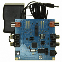
Manufacturer Part Number
QF1DA512-DK
Description
KIT DEV FOR QF1DA512
Manufacturer
Quickfilter Technologies LLC
Series
SavFIRe™r
Datasheet
1.QF1DA512-QN-T.pdf
(42 pages)
Specifications of QF1DA512-DK
Main Purpose
Filters, Digital Filter Design
Embedded
Yes, ASIC
Utilized Ic / Part
QF1Da512
Primary Attributes
1 512 Tap FIR Filter, 12 ~ 24 Bit
Secondary Attributes
Quickfilter Software Design Tool GUI, Works from 10 ~ 500ksps ADC Data Rates
For Use With
WM2582 - EVALDI EARBUDS TYPE Y686-1006 - BOARD MSP-MOJO + EXPANSION HEADR
Lead Free Status / RoHS Status
Lead free / RoHS Compliant
Other names
686-1010


The active edge of cSCK is programmable (SCLK_POL bit in the DCONFIG register) to suit the application system timing:
Sending Commands in Data Mode
If the QF1Da512 is in Data mode and it is required to reconfigure the device, it is first necessary to switch to Configure mode. This is
done by writing to the FILT_EN bit using the configuration interface.
Note: While all of the configuration registers are accessible while the QF1Da512 is in Data mode, the only registers that
should be written to are the CONFIG register FILT_EN, DIN_PT. Writes to other registers might result in corrupted filter data
or other unpredictable behavior.
In configurations in which the cSDI and the dSDI pins have been tied together, allowing for single SPI port data filtering, it is necessary
to ensure that the incoming data format does not match either the configuration register access format (see Table 4 Configuration
Register Access Format) or the FIR coefficient memory access format (see Table 2 Register and Memory Format) as this may cause
unintentional writes to configuration or coefficient memory. In other words, take care to ensure that the most significant byte of the data
input does not match either of the WRITE opcodes.
7
Modes of Operation
The QF1Da512 supports I2S or SPI and is designed to interface directly with a variety of ADC converters.
Rev A8 January 7, 2009
DATA INTERFACE
1. I2S Mode
2. SPI Mode
A word select line (WS on the dCS input) indicates which of two time-division multiplexed data channels is being
transmitted.
synchronized by a clock line (SCK on the dSCK input).
a. Normal Mode
b. Continuous Mode
c. Synchronous Serial Mode
The data is framed by the dCS input signal
Once dCS is active, data is output corresponding to clock bursts on the dSCK input
dCS is used as a trigger to indicate the start of each new sample period. dSCK runs continuously, filtered data
is output on the next n cycles of dSCK according to the programmed word length.
The channels are transmitted alternately on the data line (SD on the dSDI input) and are
Figure 4: Configuration Interface Transfer Format
sclk_pol
sclk_pol
1
0
0
1
PRELIMINARY DATA SHEET
cSDO
cSDO
cSDO
cSDO
cSCK
cSCK
cSDI
cSDI
cSDI
cSDI
z
z
z
z
13
. . .
. . .
. . .
. . .
z
z
z
z
. . .
. . .
. . .
. . .
www.quickfiltertech.com
QF1Da512
Related parts for QF1DA512-DK
Image
Part Number
Description
Manufacturer
Datasheet
Request
R

Part Number:
Description:
KIT DEV FOR QF1F512
Manufacturer:
Quickfilter Technologies LLC
Datasheet:

Part Number:
Description:
KIT DEV FOR QF4A512
Manufacturer:
Quickfilter Technologies LLC
Datasheet:

Part Number:
Description:
DEV KIT QF1D512 AUDIO MOJO
Manufacturer:
Quickfilter Technologies LLC

Part Number:
Description:
IC PROG SIGNAL CONV 4CH 32LQFP
Manufacturer:
Quickfilter Technologies LLC

Part Number:
Description:
IC FILTER DGTL PROGBL 16-VQFN
Manufacturer:
Quickfilter Technologies LLC
Datasheet:

Part Number:
Description:
IC SAVFIRE DGTL FILTER 1CH 16QFN
Manufacturer:
Quickfilter Technologies LLC

Part Number:
Description:
ADAPTER PROTOTYPING FOR QF1D512
Manufacturer:
Quickfilter Technologies LLC
Datasheet:

Part Number:
Description:
BOARD MSP-MOJO + EXPANSION HEADR
Manufacturer:
Quickfilter Technologies LLC
Datasheet:

Part Number:
Description:
ADAPTER PROG FOR QF4A512-DK
Manufacturer:
Quickfilter Technologies LLC
Datasheet:

Part Number:
Description:
REF DESIGN BLUETOOTH STER HDSET
Manufacturer:
Quickfilter Technologies LLC
Datasheet:
Part Number:
Description:
IC PROG SIGNAL CONV 4CH 32LQFP
Manufacturer:
Quickfilter Technologies LLC
Part Number:
Description:
IC FILTER DGTL PROGBL 16-VQFN
Manufacturer:
Quickfilter Technologies LLC
Datasheet:
Part Number:
Description:
IC SAVFIRE DGTL FILTER 1CH 16QFN
Manufacturer:
Quickfilter Technologies LLC