QF1DA512-DK Quickfilter Technologies LLC, QF1DA512-DK Datasheet - Page 12
QF1DA512-DK
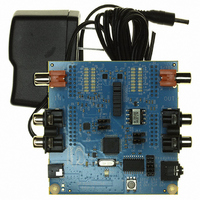
Manufacturer Part Number
QF1DA512-DK
Description
KIT DEV FOR QF1DA512
Manufacturer
Quickfilter Technologies LLC
Series
SavFIRe™r
Datasheet
1.QF1DA512-QN-T.pdf
(42 pages)
Specifications of QF1DA512-DK
Main Purpose
Filters, Digital Filter Design
Embedded
Yes, ASIC
Utilized Ic / Part
QF1Da512
Primary Attributes
1 512 Tap FIR Filter, 12 ~ 24 Bit
Secondary Attributes
Quickfilter Software Design Tool GUI, Works from 10 ~ 500ksps ADC Data Rates
For Use With
WM2582 - EVALDI EARBUDS TYPE Y686-1006 - BOARD MSP-MOJO + EXPANSION HEADR
Lead Free Status / RoHS Status
Lead free / RoHS Compliant
Other names
686-1010


6
SPI, Serial Peripheral Bus
6.1.1 Mode of Operation
The QF1Da512 is designed to interface directly with the serial peripheral interface (SPI) of microcontrollers and Digital Signal
Processors in native mode. The QF1Da512 always operates in SPI slave mode using the cSDI, cSDO, cSCK, and cCSn pins. cSDI is
the input serial data, and cSDO is the output serial data (if FILT_EN = DIN_PT = 0). cSCK is the input serial clock. Default is to
capture on rising edge, but this can be changed to capture on falling edge by writing the SCLK_POL bit in the DCONFIG register (04h).
The Control registers can be written while data is being processed.
6.1.2 Data Format
In order to address and read / write to the QF1Da512, cCSn is asserted low to select the device. When the device is in “configure”
mode but is not selected, data will not be accepted via the serial input pin (cSDI) and the serial output pin (cSDO) will remain in a high
impedance state.
Note: There are 6 “don’t care” clock cycles between the end of the op code and the 8-bit address. The value of cSDI during
these clocks has no effect on the chip. There are also two “dead” clock cycles between the end of the address input and data
output on the cSDO pin.
The Configuration SPI interface programs two different address spaces in the QF1Da512: a configuration register space and a
coefficient memory space. The configuration register space is accessed when the Op-Codes 0x82/0x83 are used (refer to the notes
above). The coefficient memory space is accessed when the Op-Codes 0x86/0x87 are used. Multiple successive registers or
coefficient values may be programmed by simply appending 8-bit data values after the first data value is written. Thus the entire
coefficient memory space may be written with a single Write access. Each 32-bit coefficient is written Most Significant Bit and Most
Significant Byte first. Each 8-bit configuration register is written Most Significant Bit first.
Rev A8 January 7, 2009
CONFIGURATION INTERFACE
cSDO
cSDO
cSCK
cCSn
cCSn
Bit #
cSDI
Bit #
cSDI
SCK
z
z
31
31
30 29 28 27 26 25 24 23 22 21 20 19 18 17 16 15 14 13 12 11 10 9 8
30 29 28 27 26 25 24 23 22 21 20 19 18 17 16 15 14 13 12 11 10 9 8
8-bit read op-code
8-bit write op-code
Figure 3: Configuration Data Timing
PRELIMINARY DATA SHEET
Notes:
> Above waveforms assume a transfer format with sclk_pol = 1
> cSDI capture edge is determined by sclk_pol setting
> cSDO transitions on opposite edge of SDI capture
> cSDO is tri-stated when cCSn is high
> Holding cCSn low continues data read/write accesses
> Read Op-Codes: Registers = 0x83, Coefficient RAMS = 0x87
> Write Op-Codes: Registers = 0x82, Coefficient RAMS = 0x86
> Registers are addressed every 1 byte (8-bits wide)
> Coefficient RAMS are addressed every 4 bytes (32-bits wide)
i.e, 0x00, 0x04, 0x08...
denotes a “don‟t care”
Configuration Interface : Read Access
Configuration Interface : Write Access
8-bit address (A0)
8-bit address (A0)
12
7 6 5 4 3 2 1 0
7 6 5 4 3 2 1 0
8-bit read data (D-A0)
8-bit write data (D-A0)
7 6 5 4 3 2 1 0
7 6 5 4 3 2 1 0
8-bit read data (D-AN)
8-bit write data (D-AN)
www.quickfiltertech.com
QF1Da512
Related parts for QF1DA512-DK
Image
Part Number
Description
Manufacturer
Datasheet
Request
R

Part Number:
Description:
KIT DEV FOR QF1F512
Manufacturer:
Quickfilter Technologies LLC
Datasheet:

Part Number:
Description:
KIT DEV FOR QF4A512
Manufacturer:
Quickfilter Technologies LLC
Datasheet:

Part Number:
Description:
DEV KIT QF1D512 AUDIO MOJO
Manufacturer:
Quickfilter Technologies LLC

Part Number:
Description:
IC PROG SIGNAL CONV 4CH 32LQFP
Manufacturer:
Quickfilter Technologies LLC

Part Number:
Description:
IC FILTER DGTL PROGBL 16-VQFN
Manufacturer:
Quickfilter Technologies LLC
Datasheet:

Part Number:
Description:
IC SAVFIRE DGTL FILTER 1CH 16QFN
Manufacturer:
Quickfilter Technologies LLC

Part Number:
Description:
ADAPTER PROTOTYPING FOR QF1D512
Manufacturer:
Quickfilter Technologies LLC
Datasheet:

Part Number:
Description:
BOARD MSP-MOJO + EXPANSION HEADR
Manufacturer:
Quickfilter Technologies LLC
Datasheet:

Part Number:
Description:
ADAPTER PROG FOR QF4A512-DK
Manufacturer:
Quickfilter Technologies LLC
Datasheet:

Part Number:
Description:
REF DESIGN BLUETOOTH STER HDSET
Manufacturer:
Quickfilter Technologies LLC
Datasheet:
Part Number:
Description:
IC PROG SIGNAL CONV 4CH 32LQFP
Manufacturer:
Quickfilter Technologies LLC
Part Number:
Description:
IC FILTER DGTL PROGBL 16-VQFN
Manufacturer:
Quickfilter Technologies LLC
Datasheet:
Part Number:
Description:
IC SAVFIRE DGTL FILTER 1CH 16QFN
Manufacturer:
Quickfilter Technologies LLC