MCP3424EV Microchip Technology, MCP3424EV Datasheet
MCP3424EV
Specifications of MCP3424EV
Available stocks


Related parts for MCP3424EV

MCP3424EV Summary of contents
Page 1
... Bridge Sensing for Pressure, Strain, and Force • Factory Automation Equipment • Consumer Goods • Weigh Scales and Fuel Gauges © 2008 Microchip Technology Inc. Description The MCP3424 is a low noise, high accuracy delta-sigma analog-to-digital (ΔΣ A/D) converter with 4 differential input channels and bits of resolu- tion ...
Page 2
... Gain = 1,2, CH4+ CH4- DS22088A-page 2 SOIC, TSSOP CH1+ CH4 CH1 CH4+ CH2 CH3- CH2- 11 CH3 Adr1 Adr0 9 DD SDA SCL Voltage Reference (2.048V) V REF ΔΣ ADC PGA Converter Interface Clock Oscillator Adr1 Adr0 SCL SDA © 2008 Microchip Technology Inc. ...
Page 3
... Addr_Float voltage is applied at address pin voltage is applied at address pin (left “floating”). © 2008 Microchip Technology Inc. †Notice: Stresses above those listed under “Maximum Rat- ings” may cause permanent damage to the device. This is a stress rating only and functional operation of the device at those or any other conditions above those indicated in the operational listings of this specification is not implied ...
Page 4
... IH µ GND IL V The device reads logic low. V The device reads logic high. V Read pin voltage if voltage is applied to the address pin. (Note 8) Device outputs float output voltage (V /2) on the address DD pin, if left “floating”. (Note © 2008 Microchip Technology Inc. ...
Page 5
... TEMPERATURE CHARACTERISTICS Electrical Specifications: Unless otherwise indicated, Parameters Temperature Ranges Specified Temperature Range Operating Temperature Range Storage Temperature Range Thermal Package Resistances Thermal Resistance, 14L-SOIC Thermal Resistance, 14L-TSSOP © 2008 Microchip Technology Inc -40°C to +125° Sym Min Typ Max Units T -40 — ...
Page 6
... PGA = 1 PGA = 8 PGA = 4 PGA = 2 -50 - 100 Input Signal (% of FSR) Output Noise vs. Input T = +25°C A PGA = 2 -50 - 100 Input Voltage (% of Full-Scale) Total Error vs. Input Voltage. PGA = 8 PGA = 1 PGA = 2 PGA = 100 120 140 Temperature (°C) Gain Error vs. Temperature. © 2008 Microchip Technology Inc. ...
Page 7
... DDS -60 -40 - 100 120 140 Temperature (°C) FIGURE 2-9: I vs. Temperature. DDB © 2008 Microchip Technology Inc. = +5.0V 0V, CHn+ = CHn Data Rate = 3.75 SPS 2. -60 -40 -20 FIGURE 2-10: Temperature. 0 -10 -20 -30 -40 -50 -60 -70 -80 -90 -100 V = 2.7V DD -110 -120 0.1 ...
Page 8
... SAMPLE 0. LEAKAGE 0. ±1 nA Leakage Current at Analog Pin LEAKAGE SS = Sampling Switch R = Sampling Switch Resistor Sample Capacitance SAMPLE “Electrical Characteristics” and is the package pin capacitance and and D are the ESD diodes Sampling Switch SAMPLE (3.2 pF) © 2008 Microchip Technology Inc. ...
Page 9
... Therefore, it needs a pull-up resistor from the V to the SCL pin. Refer to Section 5.3 “I 2 munications” for more details Serial Interface communication. © 2008 Microchip Technology Inc. ) 3.4 Serial Data Pin (SDA) SS SDA is the serial data pin of the I pin is used for input and output data. In read mode, the conversion result is read from the SDA pin (output) ...
Page 10
... The charging and discharging of the input sampling capacitor creates dynamic input currents at each input pin. The current is a function of the differen- ) tial input voltages, and inversely proportional to the DD internal sampling capacitance, frequency, and PGA setting. pin DD Figure 4-1 illustrates Time Reset © 2008 Microchip Technology Inc. ...
Page 11
... Care must be taken in setting the input voltage ranges so that the input voltage does not exceed the absolute maximum input voltage range. © 2008 Microchip Technology Inc. 4.6 Input Impedance The MCP3424 uses a switched-capacitor input stage using a 3.2 pF sampling capacitor. This capacitor is ...
Page 12
... Digital Output Code 011111111111111111 011111111111111111 000000000000000010 000000000000000001 000000000000000000 111111111111111111 111111111111111110 100000000000000000 100000000000000000 MINIMUM AND MAXIMUM OUTPUT CODES Minimum Maximum Code Code 240 SPS -2048 2047 60 SPS -8192 8191 15 SPS -32768 32767 3.75 SPS -131072 131071 N N-1 © 2008 Microchip Technology Inc. ...
Page 13
... REF ≤ -V 100000000000000000 REF Note 1: See Table 5-3 for more details of digital output codes for each conversion mode. © 2008 Microchip Technology Inc. EQUATION 4-4: CONVERTING OUTPUT CODES TO INPUT VOLTAGE If MSB = 0 (Positive Output Code): Input Voltage = (Output Code) If MSB = 1 (Negative Output Code): ′ ...
Page 14
... In this example, the device consumes approx- imately 36 µA (135 µA / 3.75 SPS = 36 µA), if the device performs only one conversion per second (1 SPS) in 18-bit conversion mode with 3V power supply © 2008 Microchip Technology Inc. ...
Page 15
... SPS (16 bits 3.75 SPS (18 bits) bit 1-0 G1-G0: PGA Gain Selection Bits (Default © 2008 Microchip Technology Inc. The user can rewrite the configuration byte any time during the device operation. configuration register bits. R/W-1 R/W-0 R/W-0 O Unimplemented bit, read as ‘0’ ...
Page 16
... Figure 5-1 shows the MCP3424 address byte. Figure 5-3 through configuration register bits and read the conversion results (Inter-Integrated and supports standard bidirectional Figure 6- bus characteristic is described 2 C address bits (A2, Figure 5-5 show how to write the © 2008 Microchip Technology Inc. ...
Page 17
... During normal operation (after the address pins are latched), the address pins are internally disabled from the rests of the internal circuit. © 2008 Microchip Technology Inc recommended to issue a General Call Reset or General Call Latch command once after the device has powered up ...
Page 18
... Float 1 (Addr_High) 0 (Addr_Low) 1 (Addr_High) Float R/W ACK by O/C MCP3424 RDY (a) One-Shot Mode: 1 (b) Continuous Mode: not effected 2nd Byte: Configuration Byte ACK by Stop Bit by MCP3424 Master © 2008 Microchip Technology Inc. ...
Page 19
... D13 is MSB (= sign bit repeated MSB of the data byte. 4: D11 is MSB (= sign bit repeated MSB of the data byte. © 2008 Microchip Technology Inc. MSB bits and can be ignored. The 5th bit (D11) of the byte represents the MSB (= sign bit) of the conversion data ...
Page 20
... MCP3424 FIGURE 5-4: Timing Diagram For Reading From The DS22088A-page 20 With 18-Bit Mode. MCP3424 © 2008 Microchip Technology Inc. ...
Page 21
... FIGURE 5-5: Timing Diagram For Reading From The MCP3424 With 12-Bit to 16-Bit Modes. © 2008 Microchip Technology Inc. MCP3424 DS22088A-page 21 ...
Page 22
... HIGH period of the clock signal. The data on the line must be changed during the LOW period of the clock signal. There is one clock pulse per bit of data. Each data transfer is initiated with a START condition and terminated with a STOP condition specification. 5-7. © 2008 Microchip Technology Inc. ...
Page 23
... START CONDITION FIGURE 5-7: Data Transfer Sequence on I © 2008 Microchip Technology Inc. During reads, the Master (microcontroller) can terminate the current read operation by not providing an acknowledge bit on the last byte that has been clocked out from the MCP3424. In this case, the ...
Page 24
... V (Note From (Note After this period, the first clock pulse is generated ns Only relevant for repeated Start condition ns (Note (Note 2, Note 3) ns Time between START and STOP conditions. ns SDA and SCL pins (Note HD:DAT ) or SU:DAT parameter. AA © 2008 Microchip Technology Inc. ...
Page 25
... Clock Low time (T ) can be affected. LOW For Data Output: This parameter is characterized, and tested indirectly by testing T 5: This parameter is ensured by characterization and not 100% tested. This parameter is not available for Standard Mode. © 2008 Microchip Technology Inc. = -40 to +85° Min Typ Max 0 — ...
Page 26
... MCP3424 SCL SU:STA T LOW T SDA HD:STA FIGURE 5- Bus Timing Data. DS22088A-page 26 T HIGH T SU:DAT T HD:DAT SU:STO T BUF 0.7V DD 0.3V DD © 2008 Microchip Technology Inc. ...
Page 27
... The pull-up resistor is typically chosen between 5 kΩ and 10 kΩ ranges for standard and fast modes, and less than 1 kΩ for high speed mode depending on the presence of bus loading capacitance. © 2008 Microchip Technology Inc. 2 6.1 ADDRESS SELECTION PINS The user can tie the Adr0 and Adr1 pins left floating ...
Page 28
... Differential Input Signal Connection: Excitation 8 9 Stop Bit (b) Single-ended Input Signal Connection: R/W Excitation MCP3424 Response Sensor FIGURE 6-4: Single-Ended Input Connections. Sensor CHn+ Input Signal CHn- MCP3424 R 1 CHn+ Input Signal R 2 CHn- MCP3424 Differential and © 2008 Microchip Technology Inc. ...
Page 29
... This results in 20.48 LSB/°C output codes. This means there are about 20 LSB output codes (or about 4.32 bits) per 1°C of change in temperature. © 2008 Microchip Technology Inc. Figure 6-5, shows an example of using the MCP3424 for multi-channel thermocouple temperature measure- ment applications ...
Page 30
... ------------------ for CH2+ and CH3+ pins and R = Voltage Divider 1 2 age). Equation 6-3 the number of output code for the full scale output of the NPP301 Pressure Sensor (NPP301 Thermistor 2 T MCU O (MASTER shows an example of calculating © 2008 Microchip Technology Inc. ...
Page 31
... The thermistor sensor is simple to use and widely used for the temperature measurement applications. It has both linear and non-linear responses over temperature range used to adjust the linear region of interest 1 for measurement. © 2008 Microchip Technology Inc. ⎞ ⎟ 100 mV ⎟ 15.625μV ⎠ ...
Page 32
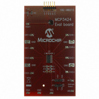
... MCP3424 Evaluation Board The MCP3424 Evaluation Board is available from Microchip Technology Inc. This board works with Micro- chip’s PICkit™ Serial Analyzer. The user can connect any sensing voltage to the input pins and read conver- sion codes using the easy-to-use PICkit™ Serial Ana- lyzer ...
Page 33
... Note: In the event the full Microchip part number cannot be marked on one line, it will be carried over to the next line, thus limiting the number of available characters for customer-specific information. © 2008 Microchip Technology Inc. MCP3424 Example: MCP3424 e ...
Page 34
... MCP3424 N NOTE DS22088A-page φ α c β © 2008 Microchip Technology Inc. ...
Page 35
... D N NOTE © 2008 Microchip Technology Inc MCP3424 φ L DS22088A-page 35 ...
Page 36
... MCP3424 NOTES: DS22088A-page 36 © 2008 Microchip Technology Inc. ...
Page 37
... APPENDIX A: REVISION HISTORY Revision A (June 2008) • Original Release of this Document. © 2008 Microchip Technology Inc. MCP3424 DS22088A-page 39 ...
Page 38
... MCP3424 NOTES: DS22088A-page 40 © 2008 Microchip Technology Inc. ...
Page 39
... MC3424T: 4-Channel 18-Bit ADC (Tape and Reel) Temperature Range -40°C to +125°C Package Plastic SOIC (150 mil Body), 14-lead ST = Plastic TSSOP (4.4mm Body), 14-lead © 2007 Microchip Technology Inc. MCP3424 Examples: a) MC3424-E/SL: 4-Channel ADC, 14LD SOIC package. b) MC3424T-E/SL: Tape and Reel, 4-Channel ADC, 14LD SOIC package ...
Page 40
... MCP3424 NOTES: DS22088A-page 42 © 2007 Microchip Technology Inc. ...
Page 41
... PowerMate, PowerTool, REAL ICE, rfLAB, Select Mode, Total Endurance, UNI/O, WiperLock and ZENA are trademarks of Microchip Technology Incorporated in the U.S.A. and other countries. SQTP is a service mark of Microchip Technology Incorporated in the U.S.A. All other trademarks mentioned herein are property of their respective companies. ...
Page 42
... Fax: 886-3-572-6459 Taiwan - Kaohsiung Tel: 886-7-536-4818 Fax: 886-7-536-4803 Taiwan - Taipei Tel: 886-2-2500-6610 Fax: 886-2-2508-0102 Thailand - Bangkok Tel: 66-2-694-1351 Fax: 66-2-694-1350 © 2008 Microchip Technology Inc. EUROPE Austria - Wels Tel: 43-7242-2244-39 Fax: 43-7242-2244-393 Denmark - Copenhagen Tel: 45-4450-2828 Fax: 45-4485-2829 France - Paris Tel: 33-1-69-53-63-20 ...