MCP3424EV Microchip Technology, MCP3424EV Datasheet - Page 15
MCP3424EV
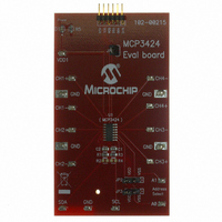
Manufacturer Part Number
MCP3424EV
Description
EVALUATION BOARD FOR MCP3424
Manufacturer
Microchip Technology
Specifications of MCP3424EV
Number Of Adc's
1
Number Of Bits
18
Sampling Rate (per Second)
3.75 ~ 240
Data Interface
I²C
Inputs Per Adc
4 Differential
Input Range
±2.048 V
Power (typ) @ Conditions
135µA @ 240sps
Voltage Supply Source
Single Supply
Operating Temperature
-55°C ~ 125°C
Utilized Ic / Part
MCP3424
Processor To Be Evaluated
MCP3424
Lead Free Status / RoHS Status
Lead free / RoHS Compliant
Lead Free Status / RoHS Status
Lead free / RoHS Compliant, Lead free / RoHS Compliant
Available stocks
Company
Part Number
Manufacturer
Quantity
Price
Company:

Part Number:
MCP3424EV
Manufacturer:
Microchip Technology
Quantity:
135


5.2
The MCP3424 has an 8-bit wide configuration register
to select for: input channel, conversion mode, conver-
sion rate, and PGA gain. This register allows the user
to change the operating condition of the device and
check the status of the device operation.
REGISTER 5-1:
© 2008 Microchip Technology Inc.
bit 7
* Default Configuration after Power-On Reset
Legend:
R = Readable bit
-n = Value at POR
bit 7
bit 6-5
bit 4
bit 3-2
bit 1-0
R/W-1
RDY
1 *
Configuration Register
RDY: Ready Bit
This bit is the data ready flag. In read mode, this bit indicates if the output register has been updated
with a latest conversion result. In One-Shot Conversion mode, writing this bit to “1” initiates a new
conversion.
Reading RDY bit with the read command:
1 = Output register has not been updated.
0 = Output register has been updated with the latest conversion result.
Writing RDY bit with the write command:
Continuous Conversion mode: No effect
One-Shot Conversion mode:
1 = Initiate a new conversion.
0 = No effect.
C1-C0: Channel Selection Bits
00 =
01 =
10 =
11 =
O/C: Conversion Mode Bit
1 = Continuous Conversion Mode (Default). The device performs data conversions continuously.
0 = One-Shot Conversion Mode. The device performs a single conversion and enters a low power
S1-S0: Sample Rate Selection Bit
00 =
01 =
10 =
11 =
G1-G0: PGA Gain Selection Bits
00 =
01 =
10 =
11 =
R/W-0
standby mode until it receives another write/read command.
C1
0 *
CONFIGURATION REGISTER
Select Channel 1 (Default)
Select Channel 2
Select Channel 3
Select Channel 4
240 SPS (12 bits) (Default)
60 SPS (14 bits)
15 SPS (16 bits)
3.75 SPS (18 bits)
x1 (Default)
x2
x4
x8
W = Writable bit
‘1’ = Bit is set
R/W-0
C0
0 *
R/W-1
O/C
1 *
‘0’ = Bit is cleared
U = Unimplemented bit, read as ‘0’
R/W-0
The user can rewrite the configuration byte any time
during the device operation.
configuration register bits.
S1
0 *
R/W-0
S0
0 *
x = Bit is unknown
R/W-0
MCP3424
Register 5-1
G1
0 *
DS22088A-page 15
shows the
R/W-0
G0
0 *
bit 0
Related parts for MCP3424EV
Image
Part Number
Description
Manufacturer
Datasheet
Request
R

Part Number:
Description:
Manufacturer:
Microchip Technology Inc.
Datasheet:
Part Number:
Description:
Manufacturer:
Microchip Technology Inc.
Datasheet:
Part Number:
Description:
Manufacturer:
Microchip Technology Inc.
Datasheet:
Part Number:
Description:
Manufacturer:
Microchip Technology Inc.
Datasheet:
Part Number:
Description:
Manufacturer:
Microchip Technology Inc.
Datasheet:
Part Number:
Description:
Manufacturer:
Microchip Technology Inc.
Datasheet:
Part Number:
Description:
Manufacturer:
Microchip Technology Inc.
Datasheet:
Part Number:
Description:
Manufacturer:
Microchip Technology Inc.
Datasheet: