MCP3424EV Microchip Technology, MCP3424EV Datasheet - Page 9
MCP3424EV
Manufacturer Part Number
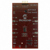
MCP3424EV
Description
EVALUATION BOARD FOR MCP3424
Manufacturer
Microchip Technology
Specifications of MCP3424EV
Number Of Adc's
1
Number Of Bits
18
Sampling Rate (per Second)
3.75 ~ 240
Data Interface
I²C
Inputs Per Adc
4 Differential
Input Range
±2.048 V
Power (typ) @ Conditions
135µA @ 240sps
Voltage Supply Source
Single Supply
Operating Temperature
-55°C ~ 125°C
Utilized Ic / Part
MCP3424
Processor To Be Evaluated
MCP3424
Lead Free Status / RoHS Status
Lead free / RoHS Compliant
Lead Free Status / RoHS Status
Lead free / RoHS Compliant, Lead free / RoHS Compliant
Available stocks
Company
Part Number
Manufacturer
Quantity
Price
Company:

Part Number:
MCP3424EV
Manufacturer:
Microchip Technology
Quantity:
135


3.2
V
requires an appropriate bypass capacitor of about
0.1 µF (ceramic) to ground. An additional 10 µF
capacitor (tantalum) in parallel is also recommended
to further attenuate high frequency noise present in
some application boards. The supply voltage (V
must be maintained in the 2.7V to 5.5V range for
specified operation.
V
device. The user must connect the V
plane through a low impedance connection. If an
analog ground path is available in the application PCB
(printed circuit board), it is highly recommended that
the V
isolated within an analog ground plane of the circuit
board.
3.3
SCL is the serial clock pin of the I
MCP3424 acts only as a slave and the SCL pin
accepts only external serial clocks. The input data
from the Master device is shifted into the SDA pin on
the rising edges of the SCL clock and output from the
MCP3424 occurs at the falling edges of the SCL clock.
The SCL pin is an open-drain N-channel driver.
Therefore, it needs a pull-up resistor from the V
to the SCL pin. Refer to Section 5.3 “I
munications” for more details of I
communication.
© 2008 Microchip Technology Inc.
DD
SS
is the ground pin and the current return path of the
is the power supply pin for the device. This pin
SS
pin be tied to the analog ground path or
Supply Voltage (V
Serial Clock Pin (SCL)
DD
2
, V
SS
2
C Serial Interface
C interface. The
2
SS
pin to a ground
C Serial Com-
)
DD
line
DD
)
3.4
SDA is the serial data pin of the I
pin is used for input and output data. In read mode, the
conversion result is read from the SDA pin (output). In
write mode, the device configuration bits are written
(input) though the SDA pin. The SDA pin is an
open-drain N-channel driver. Therefore, it needs a
pull-up resistor from the V
Except for start and stop conditions, the data on the
SDA pin must be stable during the high period of the
clock. The high or low state of the SDA pin can only
change when the clock signal on the SCL pin is low.
Refer to Section 5.3 “I
for more details of I
Typical range of the pull-up resistor value for SCL and
SDA is from 5 kΩ to 10 kΩ for standard (100 kHz) and
fast (400 kHz) modes, and less than 1 kΩ for high
speed mode (3.4 MHz).
Serial Data Pin (SDA)
2
C Serial Interface communication.
2
C Serial Communications”
DD
MCP3424
2
line to the SDA pin.
C interface. The SDA
DS22088A-page 9
Related parts for MCP3424EV
Image
Part Number
Description
Manufacturer
Datasheet
Request
R

Part Number:
Description:
Manufacturer:
Microchip Technology Inc.
Datasheet:
Part Number:
Description:
Manufacturer:
Microchip Technology Inc.
Datasheet:
Part Number:
Description:
Manufacturer:
Microchip Technology Inc.
Datasheet:
Part Number:
Description:
Manufacturer:
Microchip Technology Inc.
Datasheet:
Part Number:
Description:
Manufacturer:
Microchip Technology Inc.
Datasheet:
Part Number:
Description:
Manufacturer:
Microchip Technology Inc.
Datasheet:
Part Number:
Description:
Manufacturer:
Microchip Technology Inc.
Datasheet:
Part Number:
Description:
Manufacturer:
Microchip Technology Inc.
Datasheet: