MCP3424EV Microchip Technology, MCP3424EV Datasheet - Page 8
MCP3424EV
Manufacturer Part Number
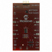
MCP3424EV
Description
EVALUATION BOARD FOR MCP3424
Manufacturer
Microchip Technology
Specifications of MCP3424EV
Number Of Adc's
1
Number Of Bits
18
Sampling Rate (per Second)
3.75 ~ 240
Data Interface
I²C
Inputs Per Adc
4 Differential
Input Range
±2.048 V
Power (typ) @ Conditions
135µA @ 240sps
Voltage Supply Source
Single Supply
Operating Temperature
-55°C ~ 125°C
Utilized Ic / Part
MCP3424
Processor To Be Evaluated
MCP3424
Lead Free Status / RoHS Status
Lead free / RoHS Compliant
Lead Free Status / RoHS Status
Lead free / RoHS Compliant, Lead free / RoHS Compliant
Available stocks
Company
Part Number
Manufacturer
Quantity
Price
Company:

Part Number:
MCP3424EV
Manufacturer:
Microchip Technology
Quantity:
135


MCP3424
3.0
The descriptions of the pins are listed in
TABLE 3-1:
3.1
CHn+ and CHn- are differential input pins for
channel n. The user can also connect CHn- pin to V
for a single-ended operation. See
ential and single-ended connection examples.
The maximum voltage range on each differential input
pin is from V
above this range will cause leakage currents through
the Electrostatic Discharge (ESD) diodes at the input
pins.
FIGURE 3-1:
DS22088A-page 8
Pin No
10
11
12
13
14
1
2
3
4
5
6
7
8
9
PIN DESCRIPTIONS
Analog Inputs (CHn+, CHn-)
SS
V
L
-0.3V to V
EGEND
R
SS
PIN FUNCTION TABLE
CHn
C
R
PIN
V
CH1+
CH2+
CH3+
CH4+
ss
CH1-
CH2-
CH3-
CH4-
Sym
Adr0
Adr1
V
SDA
SCL
V
V
T
CHn
DD
MCP3424 Analog Input Model.
SS
DD
=
=
=
=
=
+0.3V. Any voltage below or
Signal Source
Source Impedance
Analog Input Pin
Input Pin Capacitance
Threshold Voltage
Positive Differential Analog Input Pin of Channel 1
Negative Differential Analog Input Pin of Channel 1
Positive Differential Analog Input Pin of Channel 2
Negative Differential Analog Input Pin of Channel 2
Ground Pin
Positive Supply Voltage Pin
Bidirectional Serial Data Pin of the I
Serial Clock Pin of the I
I
I
Positive Differential Analog Input Pin of Channel 3
Negative Differential Analog Input Pin of Channel 3
Positive Differential Analog Input Pin of Channel 4
Negative Differential Analog Input Pin of Channel 4
2
2
C Address Selection Pin. See Section 5.3.2.
C Address Selection Pin. See Section 5.3.2.
Figure 6-4
4 pF
C
PIN
Table
D
D
1
2
V
for differ-
DD
3-1.
V
V
T
T
= 0.6V
SS
= 0.6V
2
C Interface
C
I
LEAKAGE
SAMPLE
This ESD current can cause unexpected performance
of the device. The input voltage at the input pins should
be within the specified operating range defined in
Section 1.0
Section 4.0 “Description of Device Operation”.
See Section 4.5 “Input Voltage Range” for more
details of the input voltage range.
Figure 3-1
The device uses a switched capacitor input stage at the
front end. C
typically about 4 pF. D
C
V
SAMPLE
I
(~ ±1 nA)
SS
SS
LEAKAGE
R
s
2
C Interface
Function
=
=
=
=
is the differential input sampling capacitor.
Leakage Current at Analog Pin
Sampling Switch
Sampling Switch Resistor
Sample Capacitance
shows the input structure of the MCP3424.
PIN
“Electrical
is the package pin capacitance and
SS
Sampling
Switch
1
© 2008 Microchip Technology Inc.
and D
R
S
Characteristics”
2
are the ESD diodes.
C
(3.2 pF)
SAMPLE
and
Related parts for MCP3424EV
Image
Part Number
Description
Manufacturer
Datasheet
Request
R

Part Number:
Description:
Manufacturer:
Microchip Technology Inc.
Datasheet:
Part Number:
Description:
Manufacturer:
Microchip Technology Inc.
Datasheet:
Part Number:
Description:
Manufacturer:
Microchip Technology Inc.
Datasheet:
Part Number:
Description:
Manufacturer:
Microchip Technology Inc.
Datasheet:
Part Number:
Description:
Manufacturer:
Microchip Technology Inc.
Datasheet:
Part Number:
Description:
Manufacturer:
Microchip Technology Inc.
Datasheet:
Part Number:
Description:
Manufacturer:
Microchip Technology Inc.
Datasheet:
Part Number:
Description:
Manufacturer:
Microchip Technology Inc.
Datasheet: