MCP3424EV Microchip Technology, MCP3424EV Datasheet - Page 12
MCP3424EV
Manufacturer Part Number
MCP3424EV
Description
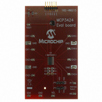
EVALUATION BOARD FOR MCP3424
Manufacturer
Microchip Technology
Specifications of MCP3424EV
Number Of Adc's
1
Number Of Bits
18
Sampling Rate (per Second)
3.75 ~ 240
Data Interface
I²C
Inputs Per Adc
4 Differential
Input Range
±2.048 V
Power (typ) @ Conditions
135µA @ 240sps
Voltage Supply Source
Single Supply
Operating Temperature
-55°C ~ 125°C
Utilized Ic / Part
MCP3424
Processor To Be Evaluated
MCP3424
Lead Free Status / RoHS Status
Lead free / RoHS Compliant
Lead Free Status / RoHS Status
Lead free / RoHS Compliant, Lead free / RoHS Compliant
Available stocks
Company
Part Number
Manufacturer
Quantity
Price
Company:

Part Number:
MCP3424EV
Manufacturer:
Microchip Technology
Quantity:
135


MCP3424
4.9
4.9.1
The digital output code is proportional to the input volt-
age and PGA settings. The output data format is a
binary two’s complement. With this code scheme, the
MSB can be considered a sign indicator. When the
MSB is a logic ‘0’, the input is positive. When the MSB
is a logic ‘1’, the input is negative. The following is an
example of the output code:
(a) for a negative full-scale input voltage: 100...000
(b) for a zero differential input voltage: 000...000
(c) for a positive full-scale input voltage: 011...111
The MSB (sign bit) is always transmitted first through
the I
sion is 18, 16, 14, or 12 bits depending on the conver-
sion rate selection bit settings by the user.
The output codes will not roll-over even if the input volt-
age exceeds the maximum input range. In this case,
the code will be locked at 0111...11 for all voltages
greater than (V
voltages less than -V
example of output codes of various input levels for 18
bit conversion mode.
minimum and maximum output codes for each conver-
sion rate option.
The number of output code is given by:
EQUATION 4-2:
The LSB of the data conversion is given by:
EQUATION 4-3:
DS22088A-page 12
Number of Output Code =
Where:
Where:
2
Example: (CHn+ - CHn-)
=
Example: (CHn+ - CHn-)
Example: (CHn+ - CHn-) = 0
C serial data line. The resolution for each conver-
See
N
(
Maximum Code
Digital Output Code and
Conversion to Real Number
Table 4-3
DIGITAL OUTPUT CODE FROM
DEVICE
=
LSB
REF
Resolution, which is set in the
Configuration Register.
=
- 1 LSB)/PGA and 1000...00 for
2 V
--------------------- -
for Maximum Code
×
Table 4-3
REF
2
+
N
REF
1
/PGA.
) PGA
×
=
•
•
2 2.048V
--------------------------
shows an example of
PGA = -2.048V
PGA = 2.048V
Table 4-2
×
×
2
(
---------------------------------------- -
N
CHn+ CHn-
2.048V
–
shows an
)
Table 4-1
setting. The measured unknown input voltage is
obtained by multiplying the output codes with LSB. See
the following section for the input voltage calculation
using the output codes.
TABLE 4-1:
TABLE 4-2:
TABLE 4-3:
Note 1:
Resolution
[CHn+ - CHn-] • PGA
Note:
Setting
Resolution Setting
12
14
16
18
Input Voltage:
2:
V
REF
shows the LSB size of each conversion rate
< -V
-1 LSB
-2 LSB
≥
- V
2 LSB
1 LSB
MSB is a sign indicator:
0: Positive input (CHn+ > CHn-)
1: Negative input (CHn+ < CHn-)
Output data format is binary two’s
complement.
Maximum n-bit code = 2
Minimum n-bit code = -1 x 2
V
12 bits
14 bits
16 bits
18 bits
- 1 LSB
0
REF
REF
REF
Data Rate
3.75 SPS
240 SPS
60 SPS
15 SPS
RESOLUTION SETTINGS VS.
LSB
EXAMPLE OF OUTPUT CODE
FOR 18 BITS
MINIMUM AND MAXIMUM
OUTPUT CODES
© 2008 Microchip Technology Inc.
Minimum
011111111111111111
011111111111111111
000000000000000010
000000000000000001
000000000000000000
111111111111111111
111111111111111110
100000000000000000
100000000000000000
-131072
-32768
Code
-2048
-8192
Digital Output Code
1 mV
250 µV
62.5 µV
15.625 µV
N-1
- 1
N-1
LSB
Maximum
131071
32767
Code
2047
8191
Related parts for MCP3424EV
Image
Part Number
Description
Manufacturer
Datasheet
Request
R

Part Number:
Description:
Manufacturer:
Microchip Technology Inc.
Datasheet:
Part Number:
Description:
Manufacturer:
Microchip Technology Inc.
Datasheet:
Part Number:
Description:
Manufacturer:
Microchip Technology Inc.
Datasheet:
Part Number:
Description:
Manufacturer:
Microchip Technology Inc.
Datasheet:
Part Number:
Description:
Manufacturer:
Microchip Technology Inc.
Datasheet:
Part Number:
Description:
Manufacturer:
Microchip Technology Inc.
Datasheet:
Part Number:
Description:
Manufacturer:
Microchip Technology Inc.
Datasheet:
Part Number:
Description:
Manufacturer:
Microchip Technology Inc.
Datasheet: