MCP3424EV Microchip Technology, MCP3424EV Datasheet - Page 10
MCP3424EV
Manufacturer Part Number
MCP3424EV
Description
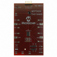
EVALUATION BOARD FOR MCP3424
Manufacturer
Microchip Technology
Specifications of MCP3424EV
Number Of Adc's
1
Number Of Bits
18
Sampling Rate (per Second)
3.75 ~ 240
Data Interface
I²C
Inputs Per Adc
4 Differential
Input Range
±2.048 V
Power (typ) @ Conditions
135µA @ 240sps
Voltage Supply Source
Single Supply
Operating Temperature
-55°C ~ 125°C
Utilized Ic / Part
MCP3424
Processor To Be Evaluated
MCP3424
Lead Free Status / RoHS Status
Lead free / RoHS Compliant
Lead Free Status / RoHS Status
Lead free / RoHS Compliant, Lead free / RoHS Compliant
Available stocks
Company
Part Number
Manufacturer
Quantity
Price
Company:

Part Number:
MCP3424EV
Manufacturer:
Microchip Technology
Quantity:
135


MCP3424
4.0
4.1
The MCP3424 is a 4-channel low-power, 18-Bit
Delta-Sigma A/D converter with an I
The device contains an input channel selection multi-
plexer (mux), a programmable gain amplifier (PGA), an
on-board voltage reference (2.048V), and an internal
oscillator.
When the device powers up (POR is set), it automati-
cally resets the configuration bits to default settings.
Device default settings are:
• Conversion bit resolution: 12 bits (240 sps)
• Input channel: Channel 1
• PGA gain setting: x1
• Continuous conversion
Once the device is powered-up, the user can repro-
gram the configuration bits using I
any time. The configuration bits are stored in volatile
memory.
User selectable options are:
• Conversion bit resolution: 12, 14, 16, or 18 bits
• Input channel selection: CH1, CH2, CH3, or CH4.
• PGA Gain selection: x1, x2, x4, or x8
• Continuous or one-shot conversion
In the Continuous Conversion mode, the device
converts the inputs continuously. While in the One-Shot
Conversion mode, the device converts the input one
time and stays in the low-power standby mode until it
receives another command for a new conversion. Dur-
ing the standby mode, the device consumes less than
1 µA maximum.
4.2
The device contains an internal Power-On-Reset
(POR) circuit that monitors power supply voltage (V
during operation. This circuit ensures correct device
start-up at system power-up and power-down events.
The device resets all configuration register bits to
default settings as soon as the POR is set.
The POR has built-in hysteresis and a timer to give a
high degree of immunity to potential ripples and noises
on the power supply. A 0.1 µF decoupling capacitor
should be mounted as close as possible to the V
for additional transient immunity.
The threshold voltage is set at 2.2V with a tolerance of
approximately ±5%. If the supply voltage falls below
this threshold, the device will be held in a reset
condition. The typical hysteresis value is approximately
200 mV.
DS22088A-page 10
DESCRIPTION OF DEVICE
OPERATION
General Overview
Power-On-Reset (POR)
2
2
C serial interface
C serial interface.
DD
DD
pin
)
The POR circuit is shut-down during the low-power
standby mode. Once a power-up event has occurred,
the device requires additional delay time (approxi-
mately 300 µs) before a conversion takes place. During
this time, all internal analog circuitries are settled
before the first conversion occurs.
the conditions for power-up and power-down events
under typical start-up conditions.
FIGURE 4-1:
4.3
The device contains an on-board 2.048V voltage
reference. This reference voltage is for internal use
only and not directly measurable. The specification of
the reference voltage is part of the device’s gain and
drift specifications. Therefore, there is no separate
specification for the on-board reference.
4.4
The user can select the input channel using the config-
uration register bits. Each channel has positive and
negative input pins. Each channel can be used for
differential or single-ended input.
Each input channel has a switched capacitor input
structure. The internal sampling capacitor (3.2 pF for
PGA = 1) is charged and discharged to process a
conversion. The charging and discharging of the input
sampling capacitor creates dynamic input currents at
each input pin. The current is a function of the differen-
tial input voltages, and inversely proportional to the
internal sampling capacitance, frequency, and PGA
setting.
V
2.2V
2.0V
DD
Reset Start-up
Internal Voltage Reference
Analog Input Channels
300 µS
Normal Operation
POR Operation.
© 2008 Microchip Technology Inc.
Figure 4-1
Reset
illustrates
Time
Related parts for MCP3424EV
Image
Part Number
Description
Manufacturer
Datasheet
Request
R

Part Number:
Description:
Manufacturer:
Microchip Technology Inc.
Datasheet:
Part Number:
Description:
Manufacturer:
Microchip Technology Inc.
Datasheet:
Part Number:
Description:
Manufacturer:
Microchip Technology Inc.
Datasheet:
Part Number:
Description:
Manufacturer:
Microchip Technology Inc.
Datasheet:
Part Number:
Description:
Manufacturer:
Microchip Technology Inc.
Datasheet:
Part Number:
Description:
Manufacturer:
Microchip Technology Inc.
Datasheet:
Part Number:
Description:
Manufacturer:
Microchip Technology Inc.
Datasheet:
Part Number:
Description:
Manufacturer:
Microchip Technology Inc.
Datasheet: