MCP3901EV-MCU16 Microchip Technology, MCP3901EV-MCU16 Datasheet - Page 15
MCP3901EV-MCU16
Manufacturer Part Number
MCP3901EV-MCU16
Description
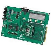
BOARD EVAL FOR 2CH ADC MCP3901
Manufacturer
Microchip Technology
Datasheets
1.MCP3901A0-ISS.pdf
(60 pages)
2.MCP3901A0-ISS.pdf
(30 pages)
3.MCP3901EV-MCU16.pdf
(38 pages)
4.MCP3901EV-MCU16.pdf
(38 pages)
Specifications of MCP3901EV-MCU16
Number Of Adc's
2
Number Of Bits
24
Data Interface
SPI™
Inputs Per Adc
1 Differential
Input Range
±1 V
Voltage Supply Source
Analog and Digital
Operating Temperature
-40°C ~ 85°C
Utilized Ic / Part
MCP3901
Silicon Manufacturer
Microchip
Application Sub Type
ADC
Kit Application Type
Data Converter
Silicon Core Number
MCP3901, PIC24F, PIC24H, DsPIC33, PIC18F86J55
Kit Contents
Board
Lead Free Status / RoHS Status
Lead free / RoHS Compliant


3.0
The descriptions of the pins are listed in
TABLE 3-1:
3.1
This pin is active low and places the entire chip in a
Reset state when active.
When RESET = 0, all registers are reset to their default
value, no communication can take place and no clock
is distributed inside the part. This state is equivalent to
a POR state.
Since the default state of the ADCs is on, the analog
power consumption when RESET = 0 is equivalent to
when RESET = 1. Only the digital power consumption
is largely reduced because this current consumption is
essentially dynamic and is reduced drastically when
there is no clock running.
All the analog biases are enabled during a Reset so
that the part is fully operational just after a RESET
rising edge.
This input is Schmitt triggered.
© 2010 Microchip Technology Inc.
Pin No.
SSOP
10
12
13
14
15
16
17
18
19
20
11
1
2
3
4
5
6
7
8
9
PIN DESCRIPTION
RESET
REFIN+/OUT
OSC1/CLKI
Symbol
RESET
REFIN-
MDAT1
MDAT0
OSC2
DV
CH0+
CH1+
AV
A
D
CH0-
CH1-
SDO
SCK
SDI
DR
CS
GND
GND
PIN FUNCTION TABLE
DD
DD
Master Reset Logic Input Pin
Digital Power Supply Pin
Analog Power Supply Pin
Non-Inverting Analog Input Pin for Channel 0
Inverting Analog Input Pin for Channel 0
Inverting Analog Input Pin for Channel 1
Non-Inverting Analog Input Pin for Channel 1
Analog Ground Pin, Return Path for Internal Analog Circuitry
Non-Inverting Voltage Reference Input and Internal Reference Output Pin
Inverting Voltage Reference Input Pin
Digital Ground Pin, Return Path for Internal Digital Circuitry
Modulator Data Output Pin for Channel 1
Modulator Data Output Pin for Channel 0
Data Ready Signal Output Pin
Oscillator Crystal Connection Pin or External Clock Input Pin
Oscillator Crystal Connection Pin
Serial Interface Chip Select Pin
Serial Interface Clock Pin
Serial Interface Data Output Pin
Serial Interface Data Input Pin
Table
3-1.
3.2
DV
within the MCP3901. This pin requires appropriate
bypass capacitors and should be maintained between
2.7V and 5.5V for specified operation.
3.3
AV
within the MCP3901.
This pin requires appropriate bypass capacitors and
should be maintained to 5V ±10% for specified
operation.
DD
DD
Function
is the power supply pin for the analog circuitry
is the power supply pin for the digital circuitry
Digital V
Analog V
DD
DD
(DV
(AV
DD
DD
MCP3901
)
)
DS22192C-page 15
Related parts for MCP3901EV-MCU16
Image
Part Number
Description
Manufacturer
Datasheet
Request
R

Part Number:
Description:
Manufacturer:
Microchip Technology Inc.
Datasheet:
Part Number:
Description:
Manufacturer:
Microchip Technology Inc.
Datasheet:
Part Number:
Description:
Manufacturer:
Microchip Technology Inc.
Datasheet:
Part Number:
Description:
Manufacturer:
Microchip Technology Inc.
Datasheet:
Part Number:
Description:
Manufacturer:
Microchip Technology Inc.
Datasheet:
Part Number:
Description:
Manufacturer:
Microchip Technology Inc.
Datasheet:
Part Number:
Description:
Manufacturer:
Microchip Technology Inc.
Datasheet:
Part Number:
Description:
Manufacturer:
Microchip Technology Inc.
Datasheet: