MCP3901EV-MCU16 Microchip Technology, MCP3901EV-MCU16 Datasheet - Page 17
MCP3901EV-MCU16
Manufacturer Part Number
MCP3901EV-MCU16
Description
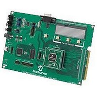
BOARD EVAL FOR 2CH ADC MCP3901
Manufacturer
Microchip Technology
Datasheets
1.MCP3901A0-ISS.pdf
(60 pages)
2.MCP3901A0-ISS.pdf
(30 pages)
3.MCP3901EV-MCU16.pdf
(38 pages)
4.MCP3901EV-MCU16.pdf
(38 pages)
Specifications of MCP3901EV-MCU16
Number Of Adc's
2
Number Of Bits
24
Data Interface
SPI™
Inputs Per Adc
1 Differential
Input Range
±1 V
Voltage Supply Source
Analog and Digital
Operating Temperature
-40°C ~ 85°C
Utilized Ic / Part
MCP3901
Silicon Manufacturer
Microchip
Application Sub Type
ADC
Kit Application Type
Data Converter
Silicon Core Number
MCP3901, PIC24F, PIC24H, DsPIC33, PIC18F86J55
Kit Contents
Board
Lead Free Status / RoHS Status
Lead free / RoHS Compliant


3.11
OSC1/CLKI and OSC2 provide the master clock for the
device. When CLKEXT = 0 (default), a resonant crystal
or clock source with a similar sinusoidal waveform must
be placed across these pins to ensure proper
operation. The typical clock frequency specified is
4 MHz. However, the clock frequency can be 1 MHz to
5 MHz without disturbing ADC accuracy. With the
current boost circuit enabled, the master clock can be
used up to 8.192 MHz without disturbing ADC
accuracy. Appropriate load capacitance should be
connected to these pins for proper operation.
3.12
This pin is the SPI chip select that enables the serial
communication.
communication can take place. A chip select falling
edge initiates the serial communication and a chip
select rising edge terminates the communication. No
communication can take place, even when CS is low
and when RESET is low.
This input is Schmitt triggered.
3.13
This is the serial clock pin for SPI communication.
Data is clocked into the device on the rising edge of
SCK. Data is clocked out of the device on the falling
edge of SCK.
The MCP3901 interface is compatible with both SPI 0,0
and 1,1 modes. SPI modes can only be changed during
a Reset.
The maximum clock speed specified is 20 MHz when
DV
This input is Schmitt triggered.
© 2010 Microchip Technology Inc.
Note:
DD
> 4.5V and 10 MHz otherwise.
Oscillator and Master Clock Input
Pins (OSC1/CLKI, OSC2)
CS (Chip Select)
SCK (Serial Data Clock)
When CLKEXT = 1, the crystal oscillator is
disabled, as well as the OSC2 input. The
OSC1 becomes the master clock input,
CLKI, the direct path for an external clock
source; for example, a clock source
generated by an MCU.
When
this
pin
is
high,
no
3.14
This is the SPI data output pin. Data is clocked out of
the device on the falling edge of SCK.
This pin stays high-impedance during the first
command byte. It also stays high-impedance during the
whole communication for write commands, and when
the CS pin is high or when the RESET pin is low. This
pin is active only when a read command is processed.
Each read is processed by a packet of 8 bits.
3.15
This is the SPI data input pin. Data is clocked into the
device on the rising edge of SCK.
When CS is low, this pin is used to communicate with a
series of 8-bit commands.
The interface is half-duplex (inputs and outputs do not
happen at the same time).
Each communication starts with a chip select falling
edge, followed by an 8-bit command word entered
through the SDI pin. Each command is either a read or
a write command. Toggling SDI during a read
command has no effect.
This input is Schmitt triggered.
SDO (Serial Data Output)
SDI (Serial Data Input)
MCP3901
DS22192C-page 17
Related parts for MCP3901EV-MCU16
Image
Part Number
Description
Manufacturer
Datasheet
Request
R

Part Number:
Description:
Manufacturer:
Microchip Technology Inc.
Datasheet:
Part Number:
Description:
Manufacturer:
Microchip Technology Inc.
Datasheet:
Part Number:
Description:
Manufacturer:
Microchip Technology Inc.
Datasheet:
Part Number:
Description:
Manufacturer:
Microchip Technology Inc.
Datasheet:
Part Number:
Description:
Manufacturer:
Microchip Technology Inc.
Datasheet:
Part Number:
Description:
Manufacturer:
Microchip Technology Inc.
Datasheet:
Part Number:
Description:
Manufacturer:
Microchip Technology Inc.
Datasheet:
Part Number:
Description:
Manufacturer:
Microchip Technology Inc.
Datasheet: