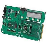
MCP3901EV-MCU16 Microchip Technology, MCP3901EV-MCU16 Datasheet - Page 46

MCP3901EV-MCU16
Manufacturer Part Number
MCP3901EV-MCU16
Description
BOARD EVAL FOR 2CH ADC MCP3901
Manufacturer
Microchip Technology
Datasheets
1.MCP3901A0-ISS.pdf
(60 pages)
2.MCP3901A0-ISS.pdf
(30 pages)
3.MCP3901EV-MCU16.pdf
(38 pages)
4.MCP3901EV-MCU16.pdf
(38 pages)
Specifications of MCP3901EV-MCU16
Number Of Adc's
2
Number Of Bits
24
Data Interface
SPI™
Inputs Per Adc
1 Differential
Input Range
±1 V
Voltage Supply Source
Analog and Digital
Operating Temperature
-40°C ~ 85°C
Utilized Ic / Part
MCP3901
Silicon Manufacturer
Microchip
Application Sub Type
ADC
Kit Application Type
Data Converter
Silicon Core Number
MCP3901, PIC24F, PIC24H, DsPIC33, PIC18F86J55
Kit Contents
Board
Lead Free Status / RoHS Status
Lead free / RoHS Compliant
MCP3901
7.5
This register contains all settings related to the
communication, including data ready settings and
status, and Read mode settings.
7.5.1
This bit determines if the first data ready pulses
correspond to settled data or unsettled data from each
SINC
every DRCLK period. If this bit is set, unsettled data will
wait for 3 DRCLK periods before giving DR pulses and
will then give DR pulses every DRCLK period.
7.5.2
This bit defines the non-active state of the data ready
pin (logic 1 or high-impedance). Using this bit, the user
can connect multiple chips with the same DR pin with a
pull-up resistor (DR_HIZN = 0) or a single chip with no
external component (DR_HIZN = 1).
7.5.3
If one of the channels is in Reset or shutdown, only one
of the data ready pulses is present and the situation is
similar to DRMODE = 01 or 10. In the ‘01’, ‘10’ and ‘11’
modes, the ADC channel data to be read is latched at
the beginning of a reading in order to prevent the case
of erroneous data when a DR pulse happens during a
read. In these modes, the two channels are
independent.
When these bits are equal to ‘11’,’10’ or ‘01’, they
control which ADC’s data ready is present on the DR
pin. When DRMODE = 00, the data ready pin output is
synchronized with the lagging ADC channel (defined by
the PHASE register) and the ADCs are linked together.
In this mode, the output of the two ADCs is latched
synchronously at the moment of the DR event. This
prevents from having bad synchronization between the
two ADCs. The output is also latched at the beginning
of a reading in order not to be updated during a read
and not to give erroneous data.
DS22192C-page 46
3
filter. Unsettled data will provide DR pulses
Status and Communication
Register
DATA READY (DR) LATENCY
CONTROL – DR_LTY
DATA READY (DR) PIN HIGH Z –
DR_HIZN
DATA READY MODE –
DRMODE<1:0>
This mode is very useful for power metering
applications because the data from both ADCs can be
retrieved, using this single data ready event, and
processed synchronously even in case of a large
phase difference. This mode works as if there was one
ADC channel and its data would be 48 bits long and
contain both channel data. As a consequence, if one
channel is in Reset or shutdown when DRMODE = 00,
no data ready pulse will be present at the outputs (if
both channels are not ready in this mode, the data is
not considered ready).
See
details about data ready pin behavior.
7.5.4
These bits indicate the DR status of both channels,
respectively. These flags are set to logic high after each
read of the STATUS/COM register. These bits are
cleared when a DR event has happened on its
respective ADC channel. Writing these bits has no
effect.
Note:
Section 6.9 “Data Ready Pin (DR)”
DR STATUS FLAG –
DRSTATUS<1:0>
These bits are useful if multiple devices
share
(DR_HIZN = 0) in order to understand
from which device the DR event has
happened. This configuration can be used
for three-phase power metering systems,
where all three phases share the same
data
DRMODE = 00 (linked ADCs), these data
ready status bits will be updated synchro-
nously upon the same event (lagging ADC
is ready). These bits are also useful in
systems where the DR pin is not used to
save MCU I/O.
ready
the
© 2010 Microchip Technology Inc.
same
pin.
DR
In
output
case
for more
the
pin


