MCP3901EV-MCU16 Microchip Technology, MCP3901EV-MCU16 Datasheet - Page 30
MCP3901EV-MCU16
Manufacturer Part Number
MCP3901EV-MCU16
Description
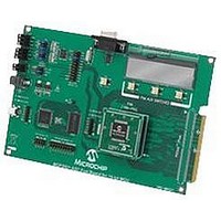
BOARD EVAL FOR 2CH ADC MCP3901
Manufacturer
Microchip Technology
Datasheets
1.MCP3901A0-ISS.pdf
(60 pages)
2.MCP3901A0-ISS.pdf
(30 pages)
3.MCP3901EV-MCU16.pdf
(38 pages)
4.MCP3901EV-MCU16.pdf
(38 pages)
Specifications of MCP3901EV-MCU16
Number Of Adc's
2
Number Of Bits
24
Data Interface
SPI™
Inputs Per Adc
1 Differential
Input Range
±1 V
Voltage Supply Source
Analog and Digital
Operating Temperature
-40°C ~ 85°C
Utilized Ic / Part
MCP3901
Silicon Manufacturer
Microchip
Application Sub Type
ADC
Kit Application Type
Data Converter
Silicon Core Number
MCP3901, PIC24F, PIC24H, DsPIC33, PIC18F86J55
Kit Contents
Board
Lead Free Status / RoHS Status
Lead free / RoHS Compliant


MCP3901
5.8
The MCP3901 contains an internal POR circuit that
monitors analog supply voltage AV
The typical threshold for a power-up event detection is
4.2V ±5%. The POR circuit has a built-in hysteresis for
improved transient spikes immunity that has a typical
value of 200 mV. Proper decoupling capacitors (0.1 µF
ceramic and 10 µF tantalum) should be mounted as
close as possible to the AV
transient immunity.
Figure 5-4
power-up and a power-down event in the typical
conditions. All internal DC biases are not settled until at
least 50 µs after system POR. Any DR pulses during
this time, after a system Reset, should be ignored. After
POR, DR pulses are present at the pin with all the
default conditions in the Configuration registers.
Both AV
Since AV
it is highly recommended to power up DV
power-up sequence. If AV
highly recommended to keep the RESET pin low during
the whole power-up sequence.
FIGURE 5-4:
DS22192C-page 30
Device
Mode
AV
4.2V
5V
4V
0V
DD
DD
Power-on Reset
DD
and DV
is the only power supply that is monitored,
illustrates the different conditions at
Reset
50 µs
DD
t
POR
power supplies are independent.
Power-on Reset Operation.
Operation
DD
DD
Proper
is powered up first, it is
pin, providing additional
DD
during operation.
Reset
DD
first as a
Time
5.9
When the RESET pin is low, both ADCs will be in Reset
and output code, 0x0000h. The RESET pin performs a
Hard Reset (DC biases still on, part ready to convert)
and clears all charges contained in the Delta-Sigma
modulators. The comparators’ output is ‘0011’ for each
ADC.
The SINC filters are all reset, as well as their double
output buffers. This pin is independent of the serial
interface. It brings the CONFIG registers to the default
state. When RESET is low, any write with the SPI
interface will be disabled and will have no effect. All
output pins (SDO, DR, MDAT0/1) are high-impedance,
and no clock is propagated through the chip.
5.10
The MCP3901 incorporates a phase delay generator
which ensures that the two ADCs are converting the
inputs with a fixed delay between them. The two ADCs
are synchronously sampling but the averaging of
modulator outputs is delayed. Therefore, the SINC filter
outputs (thus, the ADC outputs) show a fixed phase
delay, as determined by the PHASE register setting.
The PHASE register (PHASE<7:0>) is a 7 bit + sign,
MSB first, two’s complement register that indicates how
much phase delay there is to be between Channel 0
and Channel 1. The reference channel for the delay is
Channel 1 (typically the voltage channel for power
metering applications). When PHASE<7:0> are posi-
tive, Channel 0 is lagging versus Channel 1. When
PHASE<7:0> are negative, Channel 0 is leading
versus Channel 1. The amount of delay between two
ADC conversions is given by the following formula:
EQUATION 5-5:
The timing resolution of the phase delay is 1/DMCLK or
1 µs in the default configuration with MCLK = 4 MHz.
The data ready signals are affected by the phase delay
settings. Typically, the time difference between the data
ready pulses of Channel 0 and Channel 1 is equal to
the phase delay setting.
Note:
RESET Effect on Delta-Sigma
Modulator/SINC Filter
Phase Delay Block
Delay
A detailed explanation of the Data Ready
pin (DR) with phase delay is present in
Section 6.10 “Data Ready Latches and
Data Ready Modes
=
Phase Register Code
------------------------------------------------- -
© 2010 Microchip Technology Inc.
DMCLK
(DRMODE<1:0>)”.
Related parts for MCP3901EV-MCU16
Image
Part Number
Description
Manufacturer
Datasheet
Request
R

Part Number:
Description:
Manufacturer:
Microchip Technology Inc.
Datasheet:
Part Number:
Description:
Manufacturer:
Microchip Technology Inc.
Datasheet:
Part Number:
Description:
Manufacturer:
Microchip Technology Inc.
Datasheet:
Part Number:
Description:
Manufacturer:
Microchip Technology Inc.
Datasheet:
Part Number:
Description:
Manufacturer:
Microchip Technology Inc.
Datasheet:
Part Number:
Description:
Manufacturer:
Microchip Technology Inc.
Datasheet:
Part Number:
Description:
Manufacturer:
Microchip Technology Inc.
Datasheet:
Part Number:
Description:
Manufacturer:
Microchip Technology Inc.
Datasheet: