MCP3901EV-MCU16 Microchip Technology, MCP3901EV-MCU16 Datasheet - Page 47
MCP3901EV-MCU16
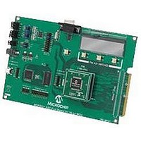
Manufacturer Part Number
MCP3901EV-MCU16
Description
BOARD EVAL FOR 2CH ADC MCP3901
Manufacturer
Microchip Technology
Datasheets
1.MCP3901A0-ISS.pdf
(60 pages)
2.MCP3901A0-ISS.pdf
(30 pages)
3.MCP3901EV-MCU16.pdf
(38 pages)
4.MCP3901EV-MCU16.pdf
(38 pages)
Specifications of MCP3901EV-MCU16
Number Of Adc's
2
Number Of Bits
24
Data Interface
SPI™
Inputs Per Adc
1 Differential
Input Range
±1 V
Voltage Supply Source
Analog and Digital
Operating Temperature
-40°C ~ 85°C
Utilized Ic / Part
MCP3901
Silicon Manufacturer
Microchip
Application Sub Type
ADC
Kit Application Type
Data Converter
Silicon Core Number
MCP3901, PIC24F, PIC24H, DsPIC33, PIC18F86J55
Kit Contents
Board
Lead Free Status / RoHS Status
Lead free / RoHS Compliant


REGISTER 7-5:
© 2010 Microchip Technology Inc.
bit 7
Legend:
R = Readable bit
-n = Value at POR
bit 7-6
bit 5
bit 4
bit 3-2
bit 1-0
READ<1> READ<0>
R/W-1
READ<1:0>: Address Loop Setting bits
11 = Address counter loops on entire register map
10 = Address counter loops on register types (default)
01 = Address counter loops on register groups
00 = Address not incremented, continually read same single register
DR_LTY: Data Ready Latency Control bit
1 = “No Latency” Conversion, DR pulses after 3 DRCLK periods (default)
0 = Unsettled Data is available after every DRCLK period
DR_HIZN: Data Ready Pin Inactive State Control bit
1 = The data ready pin default state is a logic high when data is NOT ready
0 = The data ready pin default state is high-impedance when data is NOT ready (default)
DRMODE<1:0>: Data Ready Pin (DR) Control bits
11 = Both Data Ready pulses from ADC0 and ADC Channel 1 are output on the DR pin.
10 = Data Ready pulses from ADC Channel 1 are output on the DR pin. DR from ADC Channel 0 are not
01 = Data Ready pulses from ADC Channel 0 are output on the DR pin. DR from ADC Channel 1 are not
00 = Data Ready pulses from the lagging ADC between the two are output on the DR pin. The lagging
DRSTATUS_CH<1:0>: Data Ready Status bits
11 = ADC Channel 1 and Channel 0 data is not ready (default)
10 = ADC Channel 1 data is not ready, ADC Channel 0 data is ready
01 = ADC Channel 0 data is not ready, ADC Channel 1 data is ready
00 = ADC Channel 1 and Channel 0 data is ready
R/W-0
present on the pin.
present on the pin.
ADC selection depends on the PHASE register and on the OSR (default).
STATUS AND COMMUNICATION REGISTER: ADDRESS 0x09
W = Writable bit
‘1’ = Bit is set
DR_LTY
R/W-1
DR_HIZN
R/W-0
U = Unimplemented bit, read as ‘0’
‘0’ = Bit is cleared
DRMODE<1> DRMODE<0> DRSTATUS_CH1 DRSTATUS_CH0
R/W-0
R/W-0
x = Bit is unknown
R-1
MCP3901
DS22192C-page 47
R-1
bit 0
Related parts for MCP3901EV-MCU16
Image
Part Number
Description
Manufacturer
Datasheet
Request
R

Part Number:
Description:
Manufacturer:
Microchip Technology Inc.
Datasheet:
Part Number:
Description:
Manufacturer:
Microchip Technology Inc.
Datasheet:
Part Number:
Description:
Manufacturer:
Microchip Technology Inc.
Datasheet:
Part Number:
Description:
Manufacturer:
Microchip Technology Inc.
Datasheet:
Part Number:
Description:
Manufacturer:
Microchip Technology Inc.
Datasheet:
Part Number:
Description:
Manufacturer:
Microchip Technology Inc.
Datasheet:
Part Number:
Description:
Manufacturer:
Microchip Technology Inc.
Datasheet:
Part Number:
Description:
Manufacturer:
Microchip Technology Inc.
Datasheet: