MCP3901EV-MCU16 Microchip Technology, MCP3901EV-MCU16 Datasheet - Page 31
MCP3901EV-MCU16
Manufacturer Part Number
MCP3901EV-MCU16
Description
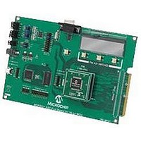
BOARD EVAL FOR 2CH ADC MCP3901
Manufacturer
Microchip Technology
Datasheets
1.MCP3901A0-ISS.pdf
(60 pages)
2.MCP3901A0-ISS.pdf
(30 pages)
3.MCP3901EV-MCU16.pdf
(38 pages)
4.MCP3901EV-MCU16.pdf
(38 pages)
Specifications of MCP3901EV-MCU16
Number Of Adc's
2
Number Of Bits
24
Data Interface
SPI™
Inputs Per Adc
1 Differential
Input Range
±1 V
Voltage Supply Source
Analog and Digital
Operating Temperature
-40°C ~ 85°C
Utilized Ic / Part
MCP3901
Silicon Manufacturer
Microchip
Application Sub Type
ADC
Kit Application Type
Data Converter
Silicon Core Number
MCP3901, PIC24F, PIC24H, DsPIC33, PIC18F86J55
Kit Contents
Board
Lead Free Status / RoHS Status
Lead free / RoHS Compliant


5.10.1
The phase delay can only go from -OSR/2 to
+OSR/2 – 1. This sets the fine phase resolution. The
PHASE register is coded with 2’s complement.
If larger delays between the two channels are needed,
they can be implemented externally to the chip with an
MCU. A FIFO in the MCU can save incoming data from
the leading channel for a number N of DRCLK clocks.
In this case, DRCLK would represent the coarse timing
resolution, and DMCLK, the fine timing resolution. The
total delay will then be equal to:
The Phase Delay register can be programmed once
with the OSR = 256 setting and will adjust to the OSR
automatically afterwards, without the need to change
the value of the PHASE register.
• OSR = 256: The delay can go from -128 to +127.
• OSR = 128: The delay can go from -64 to +63.
• OSR = 64: The delay can go from -32 to +31.
• OSR = 32: The delay can go from -16 to +15.
TABLE 5-8:
© 2010 Microchip Technology Inc.
0 1 1 1 1 1 1 1
0 1 1 1 1 1 1 0
0 0 0 0 0 0 0 1
0 0 0 0 0 0 0 0
1 1 1 1 1 1 1 1
1 0 0 0 0 0 0 1
1 0 0 0 0 0 0 0
Register Value
PHASE<7> is the sign bit, PHASE<6> is the MSB
and PHASE<0> is the LSB.
PHASE<6> is the sign bit, PHASE<5> is the MSB
and PHASE<0> is the LSB.
PHASE<5> is the sign bit, PHASE<4> is the MSB
and PHASE<0> is the LSB.
PHASE<4> is the sign bit, PHASE<3> is the MSB
and PHASE<0> is the LSB.
Delay = N/DRCLK + PHASE/DMCLK
PHASE
PHASE DELAY LIMITS
PHASE VALUES WITH
MCLK = 4 MHZ, OSR = 256
0x7F
0x7E
0xFF
0x01
0x00
0x81
0x80
Hex
(CH0 relative
to CH1)
+127 µs
+126 µs
-127 µs
-128 µs
Delay
+1 µs
-1 µs
0 µs
5.11
The MCP3901 includes a Pierce type crystal oscillator
with very high stability and ensures very low tempera-
ture and jitter for the clock generation. This oscillator
can handle up to 16.384 MHz crystal frequencies pro-
vided that proper load capacitances and the quartz
quality factor are used.
For keeping specified ADC accuracy, AMCLK should
be kept between 1 and 5 MHz with BOOST off or 1 and
8.192 MHz with BOOST on. Larger MCLK frequencies
can be used provided the prescaler clock settings allow
the AMCLK to respect these ranges.
For a proper start-up, the load capacitors of the crystal
should be connected between OSC1 and DGND, and
between OSC2 and DGND. They should also respect
the following equation:
EQUATION 5-6:
When CLKEXT = 1, the crystal oscillator is bypassed
by a digital buffer to allow direct clock input for an
external clock (see
Where:
C
LOAD
R
M
f
Crystal Oscillator
R
=
=
=
M
<
Figure
1.6 10
Crystal frequency in MHz
Load capacitance in pF including
parasitics from the PCB
Motional resistance in ohms of
the quartz
×
1-5).
6
×
MCP3901
⎛
⎝
---------------- -
C
LOAD
f
DS22192C-page 31
⎞
⎠
2
Related parts for MCP3901EV-MCU16
Image
Part Number
Description
Manufacturer
Datasheet
Request
R

Part Number:
Description:
Manufacturer:
Microchip Technology Inc.
Datasheet:
Part Number:
Description:
Manufacturer:
Microchip Technology Inc.
Datasheet:
Part Number:
Description:
Manufacturer:
Microchip Technology Inc.
Datasheet:
Part Number:
Description:
Manufacturer:
Microchip Technology Inc.
Datasheet:
Part Number:
Description:
Manufacturer:
Microchip Technology Inc.
Datasheet:
Part Number:
Description:
Manufacturer:
Microchip Technology Inc.
Datasheet:
Part Number:
Description:
Manufacturer:
Microchip Technology Inc.
Datasheet:
Part Number:
Description:
Manufacturer:
Microchip Technology Inc.
Datasheet: