CRD4525-Q1 Cirrus Logic Inc, CRD4525-Q1 Datasheet - Page 50
CRD4525-Q1
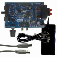
Manufacturer Part Number
CRD4525-Q1
Description
REFERENCE BOARD FOR CS4525 PWM
Manufacturer
Cirrus Logic Inc
Series
Popguard®r
Specifications of CRD4525-Q1
Amplifier Type
Class D
Output Type
2-Channel (Stereo)
Max Output Power X Channels @ Load
15W x 2 @ 8 Ohm
Voltage - Supply
12 V ~ 18 V
Operating Temperature
0°C ~ 70°C
Board Type
Fully Populated
Utilized Ic / Part
CS4525
Lead Free Status / RoHS Status
Contains lead / RoHS non-compliant
Other names
598-1586


50
6.1.9
6.1.9.1
The CS4525 includes a PWM output signal delay mechanism. This mechanism allows the PWM switching
edges to be offset between channels as a method of managing switching noise and reducing radiated
emissions.
The OutputDly[3:0] bits in the Output Cfg register are used to adjust the channel delay amount from
0 to 15 SYS_CLK or crystal input clock cycles, whichever is used as the input clock source. The absolute
delay time is calculated by multiplying the setting of the OutputDly[3:0] bits by the period of the input clock
source. By default, no delay is inserted.
When the power outputs are configured for 2-channel full-bridge operation, the OUT3/OUT4 signal pair is
delayed from the OUT1/OUT2 signal pair by the delay amount as shown in
When the power outputs are configured for 3-channel (2-channel half-bridge and 1-channel full-bridge)
operation, OUT2 is delayed from OUT1 by the delay amount, and the OUT3/OUT4 pair is delayed from
OUT2 by the delay amount as shown in
The OutputDly[3:0] bits can only be changed when all modulators and associated logic are in the power-
down state by setting the PDnAll bit. Attempts to write these bits while the PDnAll bit is cleared will be
ignored.
PWM Modulator Configuration
The CS4525 PWM modulators support flexible configuration options designed to simplify system integra-
tion. Delays may be inserted between the switching edges on adjacent channels to manage noise, and
the PWM switching frequency can be easily modified to eliminate interference with AM tuners.
Referenced Control
OutputDly[3:0] .....................
PWM Channel Delay
Figure 20. 2-Channel Full-Bridge PWM Output Delay
OUT1
OUT2
OUT3
OUT4
Register Location
“Channel Delay Settings (OutputDly[3:0])” on page 73
OUT1
OUT2
OUT3
OUT4
Figure 21. 3-Channel PWM Output Delay
tch
dly
tch
dly
tch
Figure
dly
21.
Figure
20.
CS4525
DS726PP3
Related parts for CRD4525-Q1
Image
Part Number
Description
Manufacturer
Datasheet
Request
R

Part Number:
Description:
Development Kit
Manufacturer:
Cirrus Logic Inc
Datasheet:
Part Number:
Description:
Development Kit
Manufacturer:
Cirrus Logic Inc
Datasheet:


Part Number:
Description:
High-efficiency PFC + Fluorescent Lamp Driver Reference Design
Manufacturer:
Cirrus Logic Inc
Datasheet:
Part Number:
Description:
Development Kit
Manufacturer:
Cirrus Logic Inc
Datasheet:
Part Number:
Description:
Development Kit
Manufacturer:
Cirrus Logic Inc
Datasheet:

Part Number:
Description:
Development Kit
Manufacturer:
Cirrus Logic Inc
Datasheet:
Part Number:
Description:
Development Kit
Manufacturer:
Cirrus Logic Inc
Datasheet:
Part Number:
Description:
Development Kit
Manufacturer:
Cirrus Logic Inc
Datasheet:
Part Number:
Description:
Audio Modules & Development Tools EvalBd 30W Qd Hlf- Brdg Dig Amp Pwr Stg
Manufacturer:
Cirrus Logic Inc
Datasheet:

Part Number:
Description:
EVALUATION BOARD FOR CS8427
Manufacturer:
Cirrus Logic Inc
Datasheet:

Part Number:
Description:
BOARD EVAL FOR CS8416 RCVR
Manufacturer:
Cirrus Logic Inc
Datasheet:

Part Number:
Description:
EVALUATION BOARD FOR CS8420
Manufacturer:
Cirrus Logic Inc
Datasheet:

Part Number:
Description:
KIT DEVELOPMENT EP9315 ARM9
Manufacturer:
Cirrus Logic Inc
Datasheet: