DM300023 Microchip Technology, DM300023 Datasheet - Page 176
DM300023
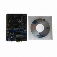
Manufacturer Part Number
DM300023
Description
KIT DEMO DSPICDEM SMPS BUCK
Manufacturer
Microchip Technology
Series
dsPIC™r
Datasheets
1.AC164335.pdf
(286 pages)
2.DM300023.pdf
(22 pages)
3.DM300023.pdf
(18 pages)
4.DM300023.pdf
(50 pages)
5.DM300023.pdf
(16 pages)
Specifications of DM300023
Main Purpose
DC/DC, Step Down
Outputs And Type
2, Non-Isolated
Voltage - Input
7 ~ 15V
Regulator Topology
Buck
Board Type
Fully Populated
Utilized Ic / Part
dsPIC30F2020
Processor To Be Evaluated
dsPIC30F202x/1010
Interface Type
RS-232
Lead Free Status / RoHS Status
Lead free / RoHS Compliant
Current - Output
-
Voltage - Output
-
Power - Output
-
Frequency - Switching
-
Lead Free Status / Rohs Status
Lead free / RoHS Compliant
Available stocks
Company
Part Number
Manufacturer
Quantity
Price
Company:

Part Number:
DM300023
Manufacturer:
Microchip Technology
Quantity:
135
Company:
Part Number:
DM300023
Manufacturer:
MICROCHIP
Quantity:
12 000


dsPIC30F1010/202X
REGISTER 16-3:
REGISTER 16-4:
DS70178C-page 174
bit 15
bit 7
Legend:
R = Readable bit
-n = Value at POR
bit 15-1
bit 0
bit 15
bit 7
Legend:
R = Readable bit
-n = Value at POR
bit 15-12
bit 11-0
Note:
PCFG7
R/W-0
R/W-0
R/W-0
U-0
—
As an alternative to using the ADBASE Register, the ADCP0-5 ADC Pair Conversion Complete Interrupts
(Interrupts 37-42) can be used to invoke A to D conversion completion routines for individual ADC input
pairs. Refer to Section 16.9 “Individual Pair Interrupts”.
ADC Base Register: This register contains the base address of the user’s ADC Interrupt Service Rou-
tine jump table. This register, when read, contains the sum of the ADBASE register contents and the
encoded value of the PxRDY Status bits.
The encoder logic provides the bit number of the highest priority PxRDY bits where P0RDY is the
highest priority, and P5RDY is lowest priority.
Unimplemented: Read as ‘0’
Unimplemented: Read as ‘0’
PCFG<11:0>: A/D Port Configuration Control bits
1 = Port pin in Digital mode, port read input enabled, A/D input multiplexor connected to AV
0 = Port pin in Analog mode, port read input disabled, A/D samples pin voltage
Note:
PCFG6
R/W-0
R/W-0
R/W-0
U-0
—
A/D BASE REGISTER (ADBASE)
A/D PORT CONFIGURATION REGISTER (ADPCFG)
The encoding results are shifted left two bits so bits 1-0 of the result are always zero.
W = Writable bit
‘1’ = Bit is set
W = Writable bit
‘1’ = Bit is set
PCFG5
R/W-0
R/W-0
R/W-0
U-0
—
ADBASE<7:1>
PCFG4
R/W-0
R/W-0
R/W-0
U-0
Preliminary
ADBASE<15:8>
—
U = Unimplemented bit, read as ‘0’
U = Unimplemented bit, read as ‘0’
‘0’ = Bit is cleared
‘0’ = Bit is cleared
PCFG11
PCFG3
R/W-0
R/W-0
R/W-0
R/W-0
PCFG10
PCFG2
R/W-0
R/W-0
R/W-0
R/W-0
© 2006 Microchip Technology Inc.
x = Bit is unknown
x = Bit is unknown
PCFG9
PCFG1
R/W-0
R/W-0
R/W-0
R/W-0
PCFG8
PCFG0
R/W-0
R/W-0
R/W-0
U-0
SS
—
bit 8
bit 0
bit 8
bit 0
Related parts for DM300023
Image
Part Number
Description
Manufacturer
Datasheet
Request
R

Part Number:
Description:
Manufacturer:
Microchip Technology Inc.
Datasheet:
Part Number:
Description:
Manufacturer:
Microchip Technology Inc.
Datasheet:
Part Number:
Description:
Manufacturer:
Microchip Technology Inc.
Datasheet:
Part Number:
Description:
Manufacturer:
Microchip Technology Inc.
Datasheet:
Part Number:
Description:
Manufacturer:
Microchip Technology Inc.
Datasheet:
Part Number:
Description:
Manufacturer:
Microchip Technology Inc.
Datasheet:
Part Number:
Description:
Manufacturer:
Microchip Technology Inc.
Datasheet:
Part Number:
Description:
Manufacturer:
Microchip Technology Inc.
Datasheet: