EVALSTSR30-60W STMicroelectronics, EVALSTSR30-60W Datasheet - Page 19
EVALSTSR30-60W
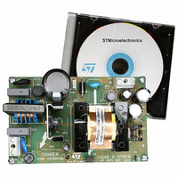
Manufacturer Part Number
EVALSTSR30-60W
Description
BOARD EVAL USING L6668 & STSR30
Manufacturer
STMicroelectronics
Type
AC/DC Switching Convertersr
Specifications of EVALSTSR30-60W
Mfg Application Notes
EVALSTSR30-60W AppNote
Main Purpose
AC/DC, Primary and Secondary Side
Outputs And Type
1, Isolated
Power - Output
60W
Voltage - Output
12V
Current - Output
5A
Voltage - Input
88 ~ 264VAC
Regulator Topology
Flyback
Frequency - Switching
68kHz
Board Type
Fully Populated
Utilized Ic / Part
L6668, STSR30
Input Voltage
88 V to 264 V
Output Voltage
12 V
Dimensions
120 mm x 75 mm
Product
Power Management Modules
Silicon Manufacturer
ST Micro
Silicon Core Number
L6668 And STSR30
Kit Application Type
Power Management - Voltage Regulator
Application Sub Type
SMPS
Kit Contents
Board
Lead Free Status / RoHS Status
Lead free / RoHS Compliant
For Use With/related Products
L6668, STSR30
Other names
497-6389
EVALSTSR30-60W
EVALSTSR30-60W
Available stocks
Company
Part Number
Manufacturer
Quantity
Price


4.7 Disable function
Latched OTP or OVP functions can be easily realized with the L6668: the IC is equipped with a compara-
tor whose non-inverting input is externally available on pin #7 (DIS), and whose inverting input is inter-
nally referenced to 2.2V.
As the voltage on the pin exceeds the threshold the IC is immediately shut down and its consumption re-
duced at a low value. The information is latched and it is necessary to let the voltage on the Vcc pin go
below the UVLO threshold to reset the latch and restart the IC.
To keep the latch supplied as long as the converter is connected to the input source, the HV generator is
activated periodically so that Vcc oscillates between the start-up threshold V
then necessary to disconnect the converter from the input source to restart the IC. This operation is shown
in the timing diagram of figure 44. Activating the HV generator in this way cuts its power dissipation ap-
proximately by three and keeps peak silicon temperature close to the average value.
4.8 Slope compensation
A pin of the device (#15, S-COMP) provides a voltage ramp during MOSFET's ON-time which is a repeti-
tion of the oscillator sawtooth, buffered (0.8 mA min. capability) and level shifted down by one Vbe.
This ramp is intended for implementing additive slope compensation on current sense. This is needed to
avoid the sub-harmonic oscillation that arises in all peak-current-mode-controlled converters working in
continuous conduction mode with a duty cycle close to or exceeding 50%.
Figure 45. Slope compensation waveforms
The compensation will be realized by connecting a programming resistor between this pin and the current
sense input (pin 12, ISEN). The pin has to be connected to the sense resistor with another resistor to make
a summing node on the pin.
Since no ramp is delivered during MOSFET OFF-time (see figure 45), no external component other than
the programming resistor is needed to ensure a clean operation at light loads. If slope compensation is
not required the pin shall be left floating.
S-COMP
S-COMP
OUT
OUT
RCT
RCT
ccON
and V
t
t
t
t
t
t
ccON
- 0.5V. It is
L6668
19/23
Related parts for EVALSTSR30-60W
Image
Part Number
Description
Manufacturer
Datasheet
Request
R

Part Number:
Description:
STMicroelectronics [RIPPLE-CARRY BINARY COUNTER/DIVIDERS]
Manufacturer:
STMicroelectronics
Datasheet:
Part Number:
Description:
STMicroelectronics [LIQUID-CRYSTAL DISPLAY DRIVERS]
Manufacturer:
STMicroelectronics
Datasheet:

Part Number:
Description:
BOARD EVAL FOR MEMS SENSORS
Manufacturer:
STMicroelectronics
Datasheet:
Part Number:
Description:
NPN TRANSISTOR POWER MODULE
Manufacturer:
STMicroelectronics
Datasheet:
Part Number:
Description:
TURBOSWITCH ULTRA-FAST HIGH VOLTAGE DIODE
Manufacturer:
STMicroelectronics
Datasheet:
Part Number:
Description:
Manufacturer:
STMicroelectronics
Datasheet:
Part Number:
Description:
DIODE / SCR MODULE
Manufacturer:
STMicroelectronics
Datasheet:
Part Number:
Description:
DIODE / SCR MODULE
Manufacturer:
STMicroelectronics
Datasheet:
Part Number:
Description:
Search -----> STE16N100
Manufacturer:
STMicroelectronics
Datasheet:
Part Number:
Description:
Search ---> STE53NA50
Manufacturer:
STMicroelectronics
Datasheet:
Part Number:
Description:
NPN Transistor Power Module
Manufacturer:
STMicroelectronics
Datasheet:
Part Number:
Description:
DIODE / SCR MODULE
Manufacturer:
STMicroelectronics
Datasheet: