EVAL-ADUC812QS Analog Devices Inc, EVAL-ADUC812QS Datasheet - Page 12
EVAL-ADUC812QS
Manufacturer Part Number
EVAL-ADUC812QS
Description
KIT DEV FOR ADUC812 QUICK START
Manufacturer
Analog Devices Inc
Series
QuickStart™ Kitr
Type
MCUr
Datasheet
1.EVAL-ADUC812QS.pdf
(60 pages)
Specifications of EVAL-ADUC812QS
Rohs Status
RoHS non-compliant
Contents
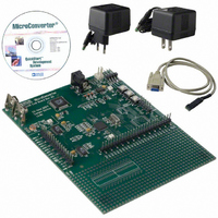
Evaluation Board, Power Supply, Cable, Software and Documentation
For Use With/related Products
ADuC812


ADuC812
ADC CIRCUIT INFORMATION
General Overview
The ADC conversion block incorporates a fast, 8-channel,
12-bit, single-supply ADC. This block provides the user with
multichannel mux, track-and-hold, on-chip reference, calibra-
tion features, and ADC. All components in this block are easily
configured via a 3-register SFR interface.
The ADC consists of a conventional successive-approximation
converter based around a capacitor DAC. The converter accepts
an analog input range of 0 V to V
and factory calibrated 2.5 V reference is provided on-chip. The
internal reference may be overdriven via the external V
This external reference can be in the range 2.3 V to AV
Single step or continuous conversion modes can be initiated in
software or alternatively by applying a convert signal to an external
pin. Timer 2 can also be configured to generate a repetitive trigger
for ADC conversions. The ADC may be configured to operate
in a DMA mode whereby the ADC block continuously converts
and captures samples to an external RAM space without any
interaction from the MCU core. This automatic capture facility
can extend through a 16 MByte external Data Memory space.
The ADuC812 is shipped with factory programmed calibration
coefficients that are automatically downloaded to the ADC on
power-up, ensuring optimum ADC performance. The ADC
core contains internal offset and gain calibration registers.
A software calibration routine is provided to allow the user to
overwrite the factory programmed calibration coefficients if
required, thus minimizing the impact of endpoint errors in the
user’s target system.
A voltage output from an on-chip band gap reference propor-
tional to absolute temperature can also be routed through the
front end ADC multiplexer (effectively a ninth ADC channel
input) facilitating a temperature sensor implementation.
REF
. A high precision, low drift
REF
DD
.
pin.
–12–
ADC Transfer Function
The analog input range for the ADC is 0 V to V
range, the designed code transitions occur midway between
successive integer LSB values (i.e., 1/2 LSB, 3/2 LSBs,
5/2 LSBs . . . FS –3/2 LSBs). The output coding is straight
binary with 1 LSB = FS/4096 or 2.5 V/4096 = 0.61 mV when
V
the 0 to V
Typical Operation
Once configured via the ADCCON 1–3 SFRs (shown on the
following page), the ADC will convert the analog input and
provide an ADC 12-bit result word in the ADCDATAH/L SFRs.
The top four bits of the ADCDATAH SFR will be written
with the channel selection bits to identify the channel result.
The format of the ADC 12-bit result word is shown in Figure 6.
REF
TOP 4 BITS
= 2.5 V. The ideal input/output transfer characteristic for
CH–ID
000...010
111...111
111...110
111...101
111...100
000...011
000...001
000...000
OUTPUT
REF
CODE
range is shown in Figure 5.
Figure 5. ADC Transfer Function
0V 1LSB
Figure 6. ADC Result Format
1LSB =
4096
FS
VOLTAGE INPUT
LOW 8 BITS OF THE
ADC RESULT WORD
HIGH 4 BITS OF
ADC RESULT WORD
ADCDATAH SFR
ADCDATAL SFR
+FS
–1LSB
REF
. For this
REV. E
Related parts for EVAL-ADUC812QS
Image
Part Number
Description
Manufacturer
Datasheet
Request
R


Part Number:
Description:
BOARD EVAL FOR SI270X-A
Manufacturer:
Silicon Laboratories Inc
Datasheet:

Part Number:
Description:
BUCK CONV REF DESIGN KIT IP1201
Manufacturer:
International Rectifier
Datasheet:
Part Number:
Description:
BOARD DEMO SYNC DUAL BUCK CNVTER
Manufacturer:
International Rectifier
Datasheet:
Part Number:
Description:
BOARD DEMO SYNC BUCK CONVETER
Manufacturer:
International Rectifier
Datasheet:

Part Number:
Description:
EVALBOARD/EB Omnidirectional microphone - Analog
Manufacturer:
Analog Devices
Datasheet:
Part Number:
Description:
EVALBOARD/EB Omnidirectional microphone - Analog
Manufacturer:
Analog Devices
Datasheet:


Part Number:
Description:
BOARD EVAL LED DRIVER LT3756
Manufacturer:
Linear Technology
Datasheet:

Part Number:
Description:
BOARD EVAL FOR AD7741/7742
Manufacturer:
Analog Devices Inc
Datasheet:

Part Number:
Description:
±1.7g Dual-Axis IMEMS Accelerometer Evaluation Board
Manufacturer:
Analog Devices Inc
Datasheet:

Part Number:
Description:
IC MULTIPLIER ANALOG 8-SOIC T/R
Manufacturer:
Analog Devices Inc
Datasheet:

Part Number:
Description:
IC ANALOG MULTIPLIER 8-DIP
Manufacturer:
Analog Devices Inc
Datasheet:
Part Number:
Description:
IC ANALOG MULTIPLIER 8-SOIC
Manufacturer:
Analog Devices Inc
Datasheet:
Part Number:
Description:
IC ANALOG MULTIPLIER 8-DIP
Manufacturer:
Analog Devices Inc
Datasheet: