EVAL-ADUC812QS Analog Devices Inc, EVAL-ADUC812QS Datasheet - Page 5
EVAL-ADUC812QS
Manufacturer Part Number
EVAL-ADUC812QS
Description
KIT DEV FOR ADUC812 QUICK START
Manufacturer
Analog Devices Inc
Series
QuickStart™ Kitr
Type
MCUr
Datasheet
1.EVAL-ADUC812QS.pdf
(60 pages)
Specifications of EVAL-ADUC812QS
Rohs Status
RoHS non-compliant
Contents
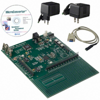
Evaluation Board, Power Supply, Cable, Software and Documentation
For Use With/related Products
ADuC812


Parameter
DIGITAL OUTPUTS
POWER REQUIREMENTS
NOTES
10
11
12
13
14
15
16
17
18
Typical specifications are not production tested, but are supported by characterization data at initial product release.
Timing Specifications—See Pages 46–55.
Specifications subject to change without notice.
Please refer to User Guide, Quick Reference Guide, Application Notes, and Silicon Errata Sheet at www.analog.com/microconverter for additional information.
REV. E
1
2
3
4
5
6
7
8
9
Specifications apply after calibration.
Temperature range –40°C to +85°C.
Linearity is guaranteed during normal MicroConverter core operation.
Linearity may degrade when programming or erasing the 640 byte Flash/EE space during ADC conversion times due to on-chip charge pump activity.
Measured in production at V
User may need to execute Software Calibration Routine to achieve these specifications, which are configuration dependent.
The offset and gain calibration spans are defined as the voltage range of user system offset and gain errors that the ADuC812 can compensate.
SNR calculation includes distortion and noise components.
Specification is not production tested, but is supported by characterization data at initial product release.
The temperature sensor will give a measure of the die temperature directly; air temperature can be inferred from this result.
DAC linearity is calculated using:
Flash/EE Memory Performance Specifications are qualified as per JEDEC Specification (Data Retention) and JEDEC Draft Specification A117 (Endurance).
Endurance Cycling is evaluated under the following conditions:
I
I
I
Analog I
EA = Port0 = DV
Reduced code range of 48 to 4095, 0 to V
Reduced code range of 48 to 3995, 0 to V
DAC output load = 10 kΩ and 50 pF.
Mode
Cycle Pattern
Erase Time
Program Time
Normal Mode (V
Normal Mode (V
Idle Mode (V
Idle Mode (V
where MCLKIN is the oscillator frequency in MHz and resultant I
DD
DD
DD
Output High Voltage (V
Output Low Voltage (V
Floating State Leakage Current
Floating State Output Capacitance
I
I
I
DD
DD
DD
ALE, PSEN, Ports 0 and 2
Port 3
at other MCLKIN frequencies is typically given by:
currents are expressed as a summation of analog and digital power supply currents during normal MicroConverter operation.
is not measured during Flash/EE program or erase cycles; I
Normal Mode
Idle Mode
Power-Down Mode
DD
= 2 mA (typ) in normal operation (internal V
DD
DD
= 5 V):
= 3 V):
DD
DD
DD
, XTAL1 (Input) tied to DV
= 5 V):
= 3 V):
= Byte Programming, Page Erase Cycling
= 00H to FFH
= 20 ms
= 100 µs
17
DD
OL
18
OH
= 5 V after Software Calibration Routine at 25°C only.
I
I
I
I
DD
DD
DD
DD
)
)
14, 15, 16
= (1.6 nAs × MCLKIN) + 6 mA
= (0.8 nAs × MCLKIN) + 3 mA
= (0.75 nAs × MCLKIN) + 6 mA
= (0.25 nAs × MCLKIN) + 3 mA
REF
DD
range
range
DD
, during this measurement.
V
2.4
4.0
0.4
0.2
0.4
0.2
±10
±1
10
43
32
26
8
25
18
15
7
30
5
REF
DD
, ADC, and DAC peripherals powered on).
= 5 V
DD
ADuC812BS
will typically increase by 10 mA during these cycles.
DD
values are in mA.
V
2.4
2.6
0.4
0.2
0.4
0.2
±10
±1
10
25
16
12
3
10
6
6
2
15
5
DD
–5–
= 3 V
Unit
V min
V typ
V max
V typ
V max
V typ
µA max
µA typ
pF typ
mA max
mA typ
mA typ
mA typ
mA max
mA typ
mA typ
mA typ
µA max
µA typ
Test Conditions/Comments
V
I
V
I
I
I
I
I
MCLKIN = 16 MHz
MCLKIN = 16 MHz
MCLKIN = 12 MHz
MCLKIN = 1 MHz
MCLKIN = 16 MHz
MCLKIN = 16 MHz
MCLKIN = 12 MHz
MCLKIN = 1 MHz
SOURCE
SOURCE
SINK
SINK
SINK
SINK
DD
DD
= 4.5 V to 5.5 V
= 2.7 V to 3.3 V
= 1.6 mA
= 1.6 mA
= 8 mA
= 8 mA
= 80 µA
= 20 µA
ADuC812
Related parts for EVAL-ADUC812QS
Image
Part Number
Description
Manufacturer
Datasheet
Request
R


Part Number:
Description:
BOARD EVAL FOR SI270X-A
Manufacturer:
Silicon Laboratories Inc
Datasheet:

Part Number:
Description:
BUCK CONV REF DESIGN KIT IP1201
Manufacturer:
International Rectifier
Datasheet:
Part Number:
Description:
BOARD DEMO SYNC DUAL BUCK CNVTER
Manufacturer:
International Rectifier
Datasheet:
Part Number:
Description:
BOARD DEMO SYNC BUCK CONVETER
Manufacturer:
International Rectifier
Datasheet:

Part Number:
Description:
EVALBOARD/EB Omnidirectional microphone - Analog
Manufacturer:
Analog Devices
Datasheet:
Part Number:
Description:
EVALBOARD/EB Omnidirectional microphone - Analog
Manufacturer:
Analog Devices
Datasheet:


Part Number:
Description:
BOARD EVAL LED DRIVER LT3756
Manufacturer:
Linear Technology
Datasheet:

Part Number:
Description:
BOARD EVAL FOR AD7741/7742
Manufacturer:
Analog Devices Inc
Datasheet:

Part Number:
Description:
±1.7g Dual-Axis IMEMS Accelerometer Evaluation Board
Manufacturer:
Analog Devices Inc
Datasheet:

Part Number:
Description:
IC MULTIPLIER ANALOG 8-SOIC T/R
Manufacturer:
Analog Devices Inc
Datasheet:

Part Number:
Description:
IC ANALOG MULTIPLIER 8-DIP
Manufacturer:
Analog Devices Inc
Datasheet:
Part Number:
Description:
IC ANALOG MULTIPLIER 8-SOIC
Manufacturer:
Analog Devices Inc
Datasheet:
Part Number:
Description:
IC ANALOG MULTIPLIER 8-DIP
Manufacturer:
Analog Devices Inc
Datasheet: