EVAL-ADUC812QS Analog Devices Inc, EVAL-ADUC812QS Datasheet - Page 41
EVAL-ADUC812QS
Manufacturer Part Number
EVAL-ADUC812QS
Description
KIT DEV FOR ADUC812 QUICK START
Manufacturer
Analog Devices Inc
Series
QuickStart™ Kitr
Type
MCUr
Datasheet
1.EVAL-ADUC812QS.pdf
(60 pages)
Specifications of EVAL-ADUC812QS
Rohs Status
RoHS non-compliant
Contents
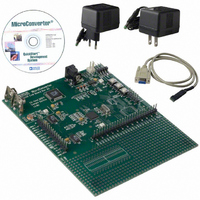
Evaluation Board, Power Supply, Cable, Software and Documentation
For Use With/related Products
ADuC812


If access to more than 64K bytes of RAM is desired, a feature
unique to the ADuC812 allows addressing up to 16 MBytes
of external RAM simply by adding an additional latch as illus-
trated in Figure 39.
In either implementation, Port 0 (P0) serves as a multiplexed
address/data bus. It emits the low byte of the data pointer (DPL) as
an address, which is latched by a pulse of ALE prior to data being
placed on the bus by the ADuC812 (write operation) or the
SRAM (read operation). Port 2 (P2) provides the data pointer
page byte (DPP) to be latched by ALE, followed by the data
pointer high byte (DPH). If no latch is connected to P2, DPP is
ignored by the SRAM and the 8051 standard of 64K byte external
data memory access is maintained.
Detailed timing diagrams of external program and data memory
read and write access can be found in the Timing Specifica-
tion sections.
Power-On Reset Operation
External POR (power-on reset) circuitry must be implemented to
drive the RESET pin of the ADuC812. The circuit must hold
the RESET pin asserted (high) whenever the power supply
(DV
2.5 V for at least 10 ms before the RESET signal is deasserted
(low), by which time the power supply must have reached at least
a 2.7 V level. The external POR circuit must be operational
down to 1.2 V or less. The timing diagram in Figure 40 illus-
trates this functionality under three separate events: power-up,
brownout, and power-down. Notice that when RESET is asserted
(high), it tracks the voltage on DV
must be adhered to through the manufacturing flow of your
ADuC812 based system as well as during its normal power-on
operation. Failure to adhere to these recommendations can
result in permanent damage to device functionality.
REV. E
Figure 39. External Data Memory Interface (16 M Bytes
Address Space)
RESET
DV
DD
DD
) is below 2.5 V. Furthermore, V
1.2V MAX
ADuC812
2.5V MIN
Figure 40. External POR Timing
ALE
WR
RD
P0
P2
10ms
MIN
LATCH
LATCH
DD
. These recommendations
10ms
MIN
DD
D0–D7
(DATA)
A0–A7
A8–A15
A16–A23
OE
WE
must remain above
SRAM
1.2V MAX
–41–
The best way to implement an external POR function to meet the
above requirements involves the use of a dedicated POR chip, such
as the ADM809/ADM810 SOT-23 packaged PORs from Analog
Devices. Recommended connection diagrams for both active high
ADM810 and active low ADM809 PORs are shown in Figure 41
and Figure 42, respectively.
Some active-low POR chips, such as the ADM809, can be used
with a manual push-button as an additional reset source as
illustrated by the dashed line connection in Figure 42.
Power Supplies
The ADuC812’s operational power supply voltage range is 2.7 V
to 5.25 V. Although the guaranteed data sheet specifications are
given only for power supplies within 2.7 V to 3.6 V or ±10% of
the nominal 5 V level, the chip will function equally well at any
power supply level between 2.7 V and 5.5 V.
Separate analog and digital power supply pins (AV
respectively) allow AV
signals often present on the system DV
you can power AV
desired, you must ensure that they remain within ±0.3 V of one
another at all times in order to avoid damaging the chip (as per the
Absolute Maximum Ratings section). Therefore it is recommended
that unless AV
you connect back-to-back Schottky diodes between them as
shown in Figure 43.
1k
Figure 43. External Dual-Supply Connections
Figure 41. External Active High POR Circuit
Figure 42. External Active Low POR Circuit
DIGITAL SUPPLY
POWER SUPPLY
0.1 F
+
–
POWER SUPPLY
OPTIONAL
MANUAL
RESET
PUSH BUTTON
DD
(ACTIVE LOW)
(ACTIVE HIGH)
10 F
and DV
DD
POR
POR
DD
and DV
to be kept relatively free of noisy digital
DD
20
34
48
35
47
21
DV
DGND
are connected directly together,
DD
DD
ADuC812
from two separate supplies if
34
48
15
20
AGND
20
34
48
15
AV
RESET
DD
DV
DD
DV
RESET
10 F
ADuC812
DD
line. However, though
ANALOG SUPPLY
DD
ADuC812
5
6
ADuC812
0.1 F
DD
+
–
and DV
DD,
Related parts for EVAL-ADUC812QS
Image
Part Number
Description
Manufacturer
Datasheet
Request
R


Part Number:
Description:
BOARD EVAL FOR SI270X-A
Manufacturer:
Silicon Laboratories Inc
Datasheet:

Part Number:
Description:
BUCK CONV REF DESIGN KIT IP1201
Manufacturer:
International Rectifier
Datasheet:
Part Number:
Description:
BOARD DEMO SYNC DUAL BUCK CNVTER
Manufacturer:
International Rectifier
Datasheet:
Part Number:
Description:
BOARD DEMO SYNC BUCK CONVETER
Manufacturer:
International Rectifier
Datasheet:

Part Number:
Description:
EVALBOARD/EB Omnidirectional microphone - Analog
Manufacturer:
Analog Devices
Datasheet:
Part Number:
Description:
EVALBOARD/EB Omnidirectional microphone - Analog
Manufacturer:
Analog Devices
Datasheet:


Part Number:
Description:
BOARD EVAL LED DRIVER LT3756
Manufacturer:
Linear Technology
Datasheet:

Part Number:
Description:
BOARD EVAL FOR AD7741/7742
Manufacturer:
Analog Devices Inc
Datasheet:

Part Number:
Description:
±1.7g Dual-Axis IMEMS Accelerometer Evaluation Board
Manufacturer:
Analog Devices Inc
Datasheet:

Part Number:
Description:
IC MULTIPLIER ANALOG 8-SOIC T/R
Manufacturer:
Analog Devices Inc
Datasheet:

Part Number:
Description:
IC ANALOG MULTIPLIER 8-DIP
Manufacturer:
Analog Devices Inc
Datasheet:
Part Number:
Description:
IC ANALOG MULTIPLIER 8-SOIC
Manufacturer:
Analog Devices Inc
Datasheet:
Part Number:
Description:
IC ANALOG MULTIPLIER 8-DIP
Manufacturer:
Analog Devices Inc
Datasheet: