EVAL-ADUC812QS Analog Devices Inc, EVAL-ADUC812QS Datasheet - Page 23
EVAL-ADUC812QS
Manufacturer Part Number
EVAL-ADUC812QS
Description
KIT DEV FOR ADUC812 QUICK START
Manufacturer
Analog Devices Inc
Series
QuickStart™ Kitr
Type
MCUr
Datasheet
1.EVAL-ADUC812QS.pdf
(60 pages)
Specifications of EVAL-ADUC812QS
Rohs Status
RoHS non-compliant
Contents
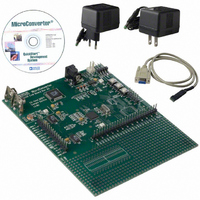
Evaluation Board, Power Supply, Cable, Software and Documentation
For Use With/related Products
ADuC812


To drive significant loads with the DAC outputs, external
buffering may be required, as illustrated in Figure 22.
The DAC output buffer also features a high impedance disable
function. In the chip’s default power-on state, both DACs are
disabled, and their outputs are in a high impedance state (or
“three-state”) where they remain inactive until enabled in software.
This means that if a zero output is desired during power-up or
power-down transient conditions, then a pull-down resistor must
be added to each DAC output. Assuming this resistor is in place,
REV. E
Figure 21. Source and Sink Current Capability with
V
REF
= V
3
2
1
0
0
Figure 22. Buffering the DAC Outputs
DD
= 3 V
SOURCE/SINK CURRENT – mA
5
10
9
10
ADuC812
15
–23–
the DAC outputs will remain at ground potential whenever the
DAC is disabled. However, each DAC output will still spike
briefly when power is first applied to the chip, and again when
each DAC is first enabled in software. Typical scope shots of
these spikes are given in Figure 23 and Figure 24, respectively.
Figure 23. DAC Output Spike at Chip Power-Up
Figure 24. DAC Output Spike at DAC Enable
5
200 s/DIV
s/DIV, 1V/DIV
DAC OUT – 500mV/DIV
AV
DD
ADuC812
– 2V/DIV
Related parts for EVAL-ADUC812QS
Image
Part Number
Description
Manufacturer
Datasheet
Request
R


Part Number:
Description:
BOARD EVAL FOR SI270X-A
Manufacturer:
Silicon Laboratories Inc
Datasheet:

Part Number:
Description:
BUCK CONV REF DESIGN KIT IP1201
Manufacturer:
International Rectifier
Datasheet:
Part Number:
Description:
BOARD DEMO SYNC DUAL BUCK CNVTER
Manufacturer:
International Rectifier
Datasheet:
Part Number:
Description:
BOARD DEMO SYNC BUCK CONVETER
Manufacturer:
International Rectifier
Datasheet:

Part Number:
Description:
EVALBOARD/EB Omnidirectional microphone - Analog
Manufacturer:
Analog Devices
Datasheet:
Part Number:
Description:
EVALBOARD/EB Omnidirectional microphone - Analog
Manufacturer:
Analog Devices
Datasheet:


Part Number:
Description:
BOARD EVAL LED DRIVER LT3756
Manufacturer:
Linear Technology
Datasheet:

Part Number:
Description:
BOARD EVAL FOR AD7741/7742
Manufacturer:
Analog Devices Inc
Datasheet:

Part Number:
Description:
±1.7g Dual-Axis IMEMS Accelerometer Evaluation Board
Manufacturer:
Analog Devices Inc
Datasheet:

Part Number:
Description:
IC MULTIPLIER ANALOG 8-SOIC T/R
Manufacturer:
Analog Devices Inc
Datasheet:

Part Number:
Description:
IC ANALOG MULTIPLIER 8-DIP
Manufacturer:
Analog Devices Inc
Datasheet:
Part Number:
Description:
IC ANALOG MULTIPLIER 8-SOIC
Manufacturer:
Analog Devices Inc
Datasheet:
Part Number:
Description:
IC ANALOG MULTIPLIER 8-DIP
Manufacturer:
Analog Devices Inc
Datasheet: