OM11035 NXP Semiconductors, OM11035 Datasheet - Page 13

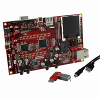
OM11035
Manufacturer Part Number
OM11035
Description
KIT EVAL LPC1768 CR
Manufacturer
NXP Semiconductors
Type
MCUr
Datasheet
1.OM11043.pdf
(79 pages)
Specifications of OM11035
Contents
Board and software
For Use With/related Products
LPC1768
Lead Free Status / RoHS Status
Lead free / RoHS Compliant
Other names
568-4815
NXP Semiconductors
Table 4.
LPC1769_68_67_66_65_64_63
Product data sheet
Symbol
P1[23]/MCI1/
PWM1[4]/MISO0
P1[24]/MCI2/
PWM1[5]/MOSI0
P1[25]/MCOA1/
MAT1[1]
P1[26]/MCOB1/
PWM1[6]/CAP0[0]
P1[27]/CLKOUT
/USB_OVRCR/
CAP0[1]
P1[28]/MCOA2/
PCAP1[0]/
MAT0[0]
P1[29]/MCOB2/
PCAP1[1]/
MAT0[1]
P1[30]/V
AD0[4]
P1[31]/SCK1/
AD0[5]
P2[0] to P2[31]
BUS
Pin description
/
Pin
37
38
39
40
43
44
45
21
20
[1]
[1]
[1]
[1]
[1]
[1]
[1]
[2]
[2]
…continued
Ball
K5
H5
G5
K6
K7
J7
G6
H1
F4
[1]
[1]
[1]
[1]
[2]
[1]
[2]
[1]
[1]
All information provided in this document is subject to legal disclaimers.
Type
I/O
I
O
I/O
I/O
I
O
I/O
I/O
O
O
I/O
O
O
I
I/O
O
I
I
I/O
O
I
O
I/O
O
I
O
I/O
I
I
I/O
I/O
I
I/O
Rev. 6.01 — 11 March 2011
Description
P1[23] — General purpose digital input/output pin.
MCI1 — Motor control PWM channel 1, input. Also Quadrature
Encoder Interface PHB input.
PWM1[4] — Pulse Width Modulator 1, channel 4 output.
MISO0 — Master In Slave Out for SSP0.
P1[24] — General purpose digital input/output pin.
MCI2 — Motor control PWM channel 2, input. Also Quadrature
Encoder Interface INDEX input.
PWM1[5] — Pulse Width Modulator 1, channel 5 output.
MOSI0 — Master Out Slave in for SSP0.
P1[25] — General purpose digital input/output pin.
MCOA1 — Motor control PWM channel 1, output A.
MAT1[1] — Match output for Timer 1, channel 1.
P1[26] — General purpose digital input/output pin.
MCOB1 — Motor control PWM channel 1, output B.
PWM1[6] — Pulse Width Modulator 1, channel 6 output.
CAP0[0] — Capture input for Timer 0, channel 0.
P1[27] — General purpose digital input/output pin.
CLKOUT — Clock output pin.
USB_OVRCR — USB port Over-Current status. (LPC1769/68/66/65
only).
CAP0[1] — Capture input for Timer 0, channel 1.
P1[28] — General purpose digital input/output pin.
MCOA2 — Motor control PWM channel 2, output A.
PCAP1[0] — Capture input for PWM1, channel 0.
MAT0[0] — Match output for Timer 0, channel 0.
P1[29] — General purpose digital input/output pin.
MCOB2 — Motor control PWM channel 2, output B.
PCAP1[1] — Capture input for PWM1, channel 1.
MAT0[1] — Match output for Timer 0, channel 1.
P1[30] — General purpose digital input/output pin.
V
(LPC1769/68/66/65/64 only).
Note: This signal must be HIGH for USB reset to occur.
AD0[4] — A/D converter 0, input 4.
P1[31] — General purpose digital input/output pin.
SCK1 — Serial Clock for SSP1.
AD0[5] — A/D converter 0, input 5.
Port 2: Port 2 is a 32-bit I/O port with individual direction controls for
each bit. The operation of port 2 pins depends upon the pin function
selected via the pin connect block. Pins 14 through 31 of this port are
not available.
BUS
— Monitors the presence of USB bus power.
LPC1769/68/67/66/65/64/63
32-bit ARM Cortex-M3 microcontroller
© NXP B.V. 2011. All rights reserved.
13 of 79


