OM11035 NXP Semiconductors, OM11035 Datasheet - Page 15
OM11035
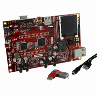
Manufacturer Part Number
OM11035
Description
KIT EVAL LPC1768 CR
Manufacturer
NXP Semiconductors
Type
MCUr
Datasheet
1.OM11043.pdf
(79 pages)
Specifications of OM11035
Contents
Board and software
For Use With/related Products
LPC1768
Lead Free Status / RoHS Status
Lead free / RoHS Compliant
Other names
568-4815


NXP Semiconductors
Table 4.
LPC1769_68_67_66_65_64_63
Product data sheet
Symbol
P2[10]/EINT0/NMI
P2[11]/EINT1/
I2STX_CLK
P2[12]/EINT2/
I2STX_WS
P2[13]/EINT3/
I2STX_SDA
P3[0] to P3[31]
P3[25]/MAT0[0]/
PWM1[2]
P3[26]/STCLK/
MAT0[1]/PWM1[3]
P4[0] to P4[31]
P4[28]/RX_MCLK/
MAT2[0]/TXD3
P4[29]/TX_MCLK/
MAT2[1]/RXD3
TDO/SWO
Pin description
Pin
53
52
51
50
27
26
82
85
1
[1][7]
[6]
[6]
[6]
[6]
[1]
[1]
[1]
[1]
…continued
Ball
J10
H8
K10
J9
H3
K1
C7
E6
A1
[6]
[1]
[1]
[1]
[6]
[1]
[1]
[6]
[6]
All information provided in this document is subject to legal disclaimers.
Type
I/O
I
I
I/O
I
I/O
I/O
I
I/O
I/O
I
I/O
I/O
I/O
O
O
I/O
I
O
O
I/O
I/O
I
O
O
I/O
I
O
I
O
O
Rev. 6.01 — 11 March 2011
Description
P2[10] — General purpose digital input/output pin. A LOW level on this
pin during reset starts the ISP command handler.
EINT0 — External interrupt 0 input.
NMI — Non-maskable interrupt input.
P2[11] — General purpose digital input/output pin.
EINT1 — External interrupt 1 input.
I2STX_CLK — Transmit Clock. It is driven by the master and received
by the slave. Corresponds to the signal SCK in the I
specification. (LPC1769/68/67/66/65/63 only).
P2[12] — General purpose digital input/output pin.
EINT2 — External interrupt 2 input.
I2STX_WS — Transmit Word Select. It is driven by the master and
received by the slave. Corresponds to the signal WS in the I
specification. (LPC1769/68/67/66/65/63 only).
P2[13] — General purpose digital input/output pin.
EINT3 — External interrupt 3 input.
I2STX_SDA — Transmit data. It is driven by the transmitter and read
by the receiver. Corresponds to the signal SD in the I
specification. (LPC1769/68/67/66/65/63 only).
Port 3: Port 3 is a 32-bit I/O port with individual direction controls for
each bit. The operation of port 3 pins depends upon the pin function
selected via the pin connect block. Pins 0 through 24, and 27 through
31 of this port are not available.
P3[25] — General purpose digital input/output pin.
MAT0[0] — Match output for Timer 0, channel 0.
PWM1[2] — Pulse Width Modulator 1, output 2.
P3[26] — General purpose digital input/output pin.
STCLK — System tick timer clock input.
MAT0[1] — Match output for Timer 0, channel 1.
PWM1[3] — Pulse Width Modulator 1, output 3.
Port 4: Port 4 is a 32-bit I/O port with individual direction controls for
each bit. The operation of port 4 pins depends upon the pin function
selected via the pin connect block. Pins 0 through 27, 30, and 31 of this
port are not available.
P4[28] — General purpose digital input/output pin.
RX_MCLK — I
MAT2[0] — Match output for Timer 2, channel 0.
TXD3 — Transmitter output for UART3.
P4[29] — General purpose digital input/output pin.
TX_MCLK — I
MAT2[1] — Match output for Timer 2, channel 1.
RXD3 — Receiver input for UART3.
TDO — Test Data out for JTAG interface.
SWO — Serial wire trace output.
LPC1769/68/67/66/65/64/63
2
2
S transmit master clock. (LPC1769/68/67/66/65 only).
S receive master clock. (LPC1769/68/67/66/65 only).
32-bit ARM Cortex-M3 microcontroller
© NXP B.V. 2011. All rights reserved.
2
S-bus
2
S-bus
2
S-bus
15 of 79
Related parts for OM11035
Image
Part Number
Description
Manufacturer
Datasheet
Request
R

Part Number:
Description:
NXP Semiconductors designed the LPC2420/2460 microcontroller around a 16-bit/32-bitARM7TDMI-S CPU core with real-time debug interfaces that include both JTAG andembedded trace
Manufacturer:
NXP Semiconductors
Datasheet:

Part Number:
Description:
NXP Semiconductors designed the LPC2458 microcontroller around a 16-bit/32-bitARM7TDMI-S CPU core with real-time debug interfaces that include both JTAG andembedded trace
Manufacturer:
NXP Semiconductors
Datasheet:
Part Number:
Description:
NXP Semiconductors designed the LPC2468 microcontroller around a 16-bit/32-bitARM7TDMI-S CPU core with real-time debug interfaces that include both JTAG andembedded trace
Manufacturer:
NXP Semiconductors
Datasheet:
Part Number:
Description:
NXP Semiconductors designed the LPC2470 microcontroller, powered by theARM7TDMI-S core, to be a highly integrated microcontroller for a wide range ofapplications that require advanced communications and high quality graphic displays
Manufacturer:
NXP Semiconductors
Datasheet:
Part Number:
Description:
NXP Semiconductors designed the LPC2478 microcontroller, powered by theARM7TDMI-S core, to be a highly integrated microcontroller for a wide range ofapplications that require advanced communications and high quality graphic displays
Manufacturer:
NXP Semiconductors
Datasheet:
Part Number:
Description:
The Philips Semiconductors XA (eXtended Architecture) family of 16-bit single-chip microcontrollers is powerful enough to easily handle the requirements of high performance embedded applications, yet inexpensive enough to compete in the market for hi
Manufacturer:
NXP Semiconductors
Datasheet:
Part Number:
Description:
The XA-S3 device is a member of Philips Semiconductors? XA(eXtended Architecture) family of high performance 16-bitsingle-chip microcontrollers
Manufacturer:
NXP Semiconductors
Datasheet:

Part Number:
Description:
The NXP BlueStreak LH75401/LH75411 family consists of two low-cost 16/32-bit System-on-Chip (SoC) devices
Manufacturer:
NXP Semiconductors
Datasheet:
Part Number:
Description:
The NXP LPC3130/3131 combine an 180 MHz ARM926EJ-S CPU core, high-speed USB2
Manufacturer:
NXP Semiconductors
Datasheet:
Part Number:
Description:
The NXP LPC3141 combine a 270 MHz ARM926EJ-S CPU core, High-speed USB 2
Manufacturer:
NXP Semiconductors
Part Number:
Description:
The NXP LPC3143 combine a 270 MHz ARM926EJ-S CPU core, High-speed USB 2
Manufacturer:
NXP Semiconductors

Part Number:
Description:
The NXP LPC3152 combines an 180 MHz ARM926EJ-S CPU core, High-speed USB 2
Manufacturer:
NXP Semiconductors
Part Number:
Description:
The NXP LPC3154 combines an 180 MHz ARM926EJ-S CPU core, High-speed USB 2
Manufacturer:
NXP Semiconductors

Part Number:
Description:
Standard level N-channel enhancement mode Field-Effect Transistor (FET) in a plastic package using NXP High-Performance Automotive (HPA) TrenchMOS technology
Manufacturer:
NXP Semiconductors
Datasheet: