C8051F700DK Silicon Laboratories Inc, C8051F700DK Datasheet - Page 180
C8051F700DK
Manufacturer Part Number
C8051F700DK
Description
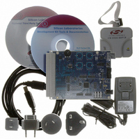
DEV KIT FOR C8051F700
Manufacturer
Silicon Laboratories Inc
Type
MCUr
Datasheets
1.C8051F700-TB.pdf
(1 pages)
2.C8051F700-TB.pdf
(306 pages)
3.C8051F700-TB.pdf
(18 pages)
Specifications of C8051F700DK
Contents
Board, Cables, CD, Debugger, Power Supply
Processor To Be Evaluated
C8051F7x
Processor Series
C8051F7xx
Interface Type
USB
Operating Supply Voltage
3.3 V
Lead Free Status / RoHS Status
Lead free / RoHS Compliant
For Use With/related Products
C8051F7xx
Lead Free Status / Rohs Status
Lead free / RoHS Compliant
Other names
336-1635


C8051F70x/71x
28. Port Input/Output
Digital and analog resources are available through 64 I/O pins. Each of the Port pins P0.0–P2.7 can be
defined as general-purpose I/O (GPIO), assigned to one of the internal digital resources, or assigned to an
analog function as shown in Figure 28.4. The designer has complete control over which functions are
assigned, limited only by the number of physical I/O pins. This resource assignment flexibility is achieved
through the use of a Priority Crossbar Decoder. The state of a Port I/O pin can always be read in the corre-
sponding Port latch, regardless of the Crossbar settings.
The Crossbar assigns the selected internal digital resources to the I/O pins based on the Priority Decoder.
The registers XBR0 and XBR1, defined in SFR Definition 28.1 and SFR Definition 28.2, are used to select
internal digital functions.
All Port I/Os except P0.3 are tolerant of voltages up to 2 V above the V
the Port cell circuit). The Port I/O cells are configured as either push-pull or open-drain in the Port Output
Mode registers (PnMDOUT, where n = 0,1). Complete Electrical Specifications for Port I/O are given in
Section “9. Electrical Characteristics” on page 47.
180
H ighest
P riority
Low est
P riority
S Y SC LK
O utputs
SM Bus
T0, T1
U AR T
P 0
P 1
PC A
C P0
S PI
(P0.0-P 0.7)
(P1.0-P 1.7)
Figure 28.1. Port I/O Functional Block Diagram
2
4
2
2
4
2
8
8
(A D C 0, C P0, V R E F, XTAL)
To Analog Peripherals
Rev. 1.0
P nS K IP R egisters
X BR 0, XB R1,
C rossbar
Decoder
Priority
Digital
To C S0
8
8
8
P 0M AS K , P0M A T
P 1M AS K , P1M A T
Port M atch
DD
C ells
C ells
C ells
C ells
C ells
C ells
C ells
supply (refer to Figure 28.2 for
I/O
I/O
I/O
I/O
I/O
I/O
P1
I/O
P 2
P3
P4
P5
P 6
P0
External Interrupts
PnM D IN , P nD R V
EX0 and E X1
PnM D O U T,
R egisters
P4.0
P4.7
P5.0
P5.7
P0.0
P0.7
P1.0
P1.7
P2.0
P2.7
P3.0
P3.7
P6.0
P6.5
Related parts for C8051F700DK
Image
Part Number
Description
Manufacturer
Datasheet
Request
R

Part Number:
Description:
SMD/C°/SINGLE-ENDED OUTPUT SILICON OSCILLATOR
Manufacturer:
Silicon Laboratories Inc
Part Number:
Description:
Manufacturer:
Silicon Laboratories Inc
Datasheet:
Part Number:
Description:
N/A N/A/SI4010 AES KEYFOB DEMO WITH LCD RX
Manufacturer:
Silicon Laboratories Inc
Datasheet:
Part Number:
Description:
N/A N/A/SI4010 SIMPLIFIED KEY FOB DEMO WITH LED RX
Manufacturer:
Silicon Laboratories Inc
Datasheet:
Part Number:
Description:
N/A/-40 TO 85 OC/EZLINK MODULE; F930/4432 HIGH BAND (REV E/B1)
Manufacturer:
Silicon Laboratories Inc
Part Number:
Description:
EZLink Module; F930/4432 Low Band (rev e/B1)
Manufacturer:
Silicon Laboratories Inc
Part Number:
Description:
I°/4460 10 DBM RADIO TEST CARD 434 MHZ
Manufacturer:
Silicon Laboratories Inc
Part Number:
Description:
I°/4461 14 DBM RADIO TEST CARD 868 MHZ
Manufacturer:
Silicon Laboratories Inc
Part Number:
Description:
I°/4463 20 DBM RFSWITCH RADIO TEST CARD 460 MHZ
Manufacturer:
Silicon Laboratories Inc
Part Number:
Description:
I°/4463 20 DBM RADIO TEST CARD 868 MHZ
Manufacturer:
Silicon Laboratories Inc
Part Number:
Description:
I°/4463 27 DBM RADIO TEST CARD 868 MHZ
Manufacturer:
Silicon Laboratories Inc
Part Number:
Description:
I°/4463 SKYWORKS 30 DBM RADIO TEST CARD 915 MHZ
Manufacturer:
Silicon Laboratories Inc
Part Number:
Description:
N/A N/A/-40 TO 85 OC/4463 RFMD 30 DBM RADIO TEST CARD 915 MHZ
Manufacturer:
Silicon Laboratories Inc
Part Number:
Description:
I°/4463 20 DBM RADIO TEST CARD 169 MHZ
Manufacturer:
Silicon Laboratories Inc