C8051F700DK Silicon Laboratories Inc, C8051F700DK Datasheet - Page 54
C8051F700DK
Manufacturer Part Number
C8051F700DK
Description
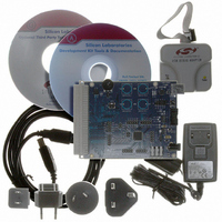
DEV KIT FOR C8051F700
Manufacturer
Silicon Laboratories Inc
Type
MCUr
Datasheets
1.C8051F700-TB.pdf
(1 pages)
2.C8051F700-TB.pdf
(306 pages)
3.C8051F700-TB.pdf
(18 pages)
Specifications of C8051F700DK
Contents
Board, Cables, CD, Debugger, Power Supply
Processor To Be Evaluated
C8051F7x
Processor Series
C8051F7xx
Interface Type
USB
Operating Supply Voltage
3.3 V
Lead Free Status / RoHS Status
Lead free / RoHS Compliant
For Use With/related Products
C8051F7xx
Lead Free Status / Rohs Status
Lead free / RoHS Compliant
Other names
336-1635


C8051F70x/71x
Table 9.14. Comparator Electrical Characteristics
V
54
Parameter
Response Time:
Mode 0, Vcm
Response Time:
Mode 1, Vcm
Response Time:
Mode 2, Vcm
Response Time:
Mode 3, Vcm
Common-Mode Rejection Ratio
Positive Hysteresis 1
Positive Hysteresis 2
Positive Hysteresis 3
Positive Hysteresis 4
Negative Hysteresis 1
Negative Hysteresis 2
Negative Hysteresis 3
Negative Hysteresis 4
Inverting or Non-Inverting Input
Voltage Range
Input Offset Voltage
Power Specifications
Power Supply Rejection
Powerup Time
Supply Current at DC
Note: Vcm is the common-mode voltage on CP0+ and CP0–.
DD
= 3.0 V, –40 to +85 °C unless otherwise noted.
*
*
*
*
= 1.5 V
= 1.5 V
= 1.5 V
= 1.5 V
Mode 2, CP0HYN1–0 = 00
Mode 2, CP0HYN1–0 = 01
Mode 2, CP0HYN1–0 = 10
Mode 2, CP0HYP1–0 = 00
Mode 2, CP0HYP1–0 = 01
Mode 2, CP0HYP1–0 = 10
Mode 2, CP0HYP1–0 = 11
Mode 2, CP0HYN1–0 = 11
CP0+ – CP0– = –100 mV
CP0+ – CP0– = –100 mV
CP0+ – CP0– = –100 mV
CP0+ – CP0– = –100 mV
CP0+ – CP0– = 100 mV
CP0+ – CP0– = 100 mV
CP0+ – CP0– = 100 mV
CP0+ – CP0– = 100 mV
Conditions
Mode 0
Mode 1
Mode 2
Mode 3
Rev. 1.0
–0.25
–7.5
Min
10
10
—
—
—
—
—
—
—
—
—
—
—
—
—
—
—
—
—
2
7
2
7
1500
4500
Typ
300
200
400
350
570
870
0.1
0.5
10
20
10
20
10
25
10
—
—
1
3
0
5
0
5
V
DD
Max
7.5
20
30
—
—
—
—
—
—
—
—
10
30
10
20
—
—
—
—
—
—
+ 0.25
4
1
1
Units
mV/V
mV/V
mV
mV
mV
mV
mV
mV
mV
mV
mV
µA
µA
µA
µA
ns
ns
ns
ns
ns
ns
ns
ns
µs
V
Related parts for C8051F700DK
Image
Part Number
Description
Manufacturer
Datasheet
Request
R

Part Number:
Description:
SMD/C°/SINGLE-ENDED OUTPUT SILICON OSCILLATOR
Manufacturer:
Silicon Laboratories Inc
Part Number:
Description:
Manufacturer:
Silicon Laboratories Inc
Datasheet:
Part Number:
Description:
N/A N/A/SI4010 AES KEYFOB DEMO WITH LCD RX
Manufacturer:
Silicon Laboratories Inc
Datasheet:
Part Number:
Description:
N/A N/A/SI4010 SIMPLIFIED KEY FOB DEMO WITH LED RX
Manufacturer:
Silicon Laboratories Inc
Datasheet:
Part Number:
Description:
N/A/-40 TO 85 OC/EZLINK MODULE; F930/4432 HIGH BAND (REV E/B1)
Manufacturer:
Silicon Laboratories Inc
Part Number:
Description:
EZLink Module; F930/4432 Low Band (rev e/B1)
Manufacturer:
Silicon Laboratories Inc
Part Number:
Description:
I°/4460 10 DBM RADIO TEST CARD 434 MHZ
Manufacturer:
Silicon Laboratories Inc
Part Number:
Description:
I°/4461 14 DBM RADIO TEST CARD 868 MHZ
Manufacturer:
Silicon Laboratories Inc
Part Number:
Description:
I°/4463 20 DBM RFSWITCH RADIO TEST CARD 460 MHZ
Manufacturer:
Silicon Laboratories Inc
Part Number:
Description:
I°/4463 20 DBM RADIO TEST CARD 868 MHZ
Manufacturer:
Silicon Laboratories Inc
Part Number:
Description:
I°/4463 27 DBM RADIO TEST CARD 868 MHZ
Manufacturer:
Silicon Laboratories Inc
Part Number:
Description:
I°/4463 SKYWORKS 30 DBM RADIO TEST CARD 915 MHZ
Manufacturer:
Silicon Laboratories Inc
Part Number:
Description:
N/A N/A/-40 TO 85 OC/4463 RFMD 30 DBM RADIO TEST CARD 915 MHZ
Manufacturer:
Silicon Laboratories Inc
Part Number:
Description:
I°/4463 20 DBM RADIO TEST CARD 169 MHZ
Manufacturer:
Silicon Laboratories Inc