C8051T610DK Silicon Laboratories Inc, C8051T610DK Datasheet - Page 110
C8051T610DK
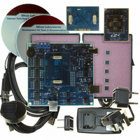
Manufacturer Part Number
C8051T610DK
Description
KIT DEV FOR C8051T61X MCU'S
Manufacturer
Silicon Laboratories Inc
Type
MCUr
Specifications of C8051T610DK
Contents
Board, daughter boards, power adapter, cables, documentation and software
Processor To Be Evaluated
C8051T61x
Interface Type
USB
Lead Free Status / RoHS Status
Lead free / RoHS Compliant
For Use With/related Products
C8051T610
For Use With
336-1507 - DAUGHTER BOARD T610 24QFN SOCKET336-1506 - DAUGHTER BOARD T610 28QFN SOCKET336-1505 - DAUGHT BOARD T610 32TQFP SOCKET
Lead Free Status / Rohs Status
Lead free / RoHS Compliant
Other names
336-1443


C8051T610/1/2/3/4/5/6/7
20.3. External Oscillator Drive Circuit
The external oscillator circuit may drive an external capacitor or RC network. A CMOS clock may also pro-
vide a clock input. In RC, capacitor, or CMOS clock configuration, the clock source should be wired to the
EXTCLK pin as shown in Figure 20.1. The type of external oscillator must be selected in the OSCXCN reg-
ister, and the frequency control bits (XFCN) must be selected appropriately (see SFR Definition 20.4).
Important Note on External Oscillator Usage: Port pins must be configured when using the external
oscillator circuit. When the external oscillator drive circuit is enabled in capacitor, RC, or CMOS clock
mode, Port pin P0.3 is used as EXTCLK. The Port I/O Crossbar should be configured to skip the Port pin
used by the oscillator circuit; see Section “21.3. Priority Crossbar Decoder” on page 117 for Crossbar con-
figuration. Additionally, when using the external oscillator circuit in capacitor or RC mode, the associated
Port pin should be configured as an analog input. In CMOS clock mode, the associated pin should be
configured as a digital input. See Section “21.4. Port I/O Initialization” on page 121 for details on Port
input mode selection.
110
Rev 1.0
Related parts for C8051T610DK
Image
Part Number
Description
Manufacturer
Datasheet
Request
R

Part Number:
Description:
SMD/C°/SINGLE-ENDED OUTPUT SILICON OSCILLATOR
Manufacturer:
Silicon Laboratories Inc
Part Number:
Description:
Manufacturer:
Silicon Laboratories Inc
Datasheet:
Part Number:
Description:
N/A N/A/SI4010 AES KEYFOB DEMO WITH LCD RX
Manufacturer:
Silicon Laboratories Inc
Datasheet:
Part Number:
Description:
N/A N/A/SI4010 SIMPLIFIED KEY FOB DEMO WITH LED RX
Manufacturer:
Silicon Laboratories Inc
Datasheet:
Part Number:
Description:
N/A/-40 TO 85 OC/EZLINK MODULE; F930/4432 HIGH BAND (REV E/B1)
Manufacturer:
Silicon Laboratories Inc
Part Number:
Description:
EZLink Module; F930/4432 Low Band (rev e/B1)
Manufacturer:
Silicon Laboratories Inc
Part Number:
Description:
I°/4460 10 DBM RADIO TEST CARD 434 MHZ
Manufacturer:
Silicon Laboratories Inc
Part Number:
Description:
I°/4461 14 DBM RADIO TEST CARD 868 MHZ
Manufacturer:
Silicon Laboratories Inc
Part Number:
Description:
I°/4463 20 DBM RFSWITCH RADIO TEST CARD 460 MHZ
Manufacturer:
Silicon Laboratories Inc
Part Number:
Description:
I°/4463 20 DBM RADIO TEST CARD 868 MHZ
Manufacturer:
Silicon Laboratories Inc
Part Number:
Description:
I°/4463 27 DBM RADIO TEST CARD 868 MHZ
Manufacturer:
Silicon Laboratories Inc
Part Number:
Description:
I°/4463 SKYWORKS 30 DBM RADIO TEST CARD 915 MHZ
Manufacturer:
Silicon Laboratories Inc
Part Number:
Description:
N/A N/A/-40 TO 85 OC/4463 RFMD 30 DBM RADIO TEST CARD 915 MHZ
Manufacturer:
Silicon Laboratories Inc
Part Number:
Description:
I°/4463 20 DBM RADIO TEST CARD 169 MHZ
Manufacturer:
Silicon Laboratories Inc