C8051T610DK Silicon Laboratories Inc, C8051T610DK Datasheet - Page 8
C8051T610DK
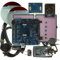
Manufacturer Part Number
C8051T610DK
Description
KIT DEV FOR C8051T61X MCU'S
Manufacturer
Silicon Laboratories Inc
Type
MCUr
Specifications of C8051T610DK
Contents
Board, daughter boards, power adapter, cables, documentation and software
Processor To Be Evaluated
C8051T61x
Interface Type
USB
Lead Free Status / RoHS Status
Lead free / RoHS Compliant
For Use With/related Products
C8051T610
For Use With
336-1507 - DAUGHTER BOARD T610 24QFN SOCKET336-1506 - DAUGHTER BOARD T610 28QFN SOCKET336-1505 - DAUGHT BOARD T610 32TQFP SOCKET
Lead Free Status / Rohs Status
Lead free / RoHS Compliant
Other names
336-1443


C8051T610/1/2/3/4/5/6/7
19. Reset Sources
20. Oscillators and Clock Selection
21. Port Input/Output
22. SMBus
23. UART0
24. Enhanced Serial Peripheral Interface (SPI0)
25. Timers
8
Figure 19.1. Reset Sources ................................................................................... 100
Figure 19.2. Power-On and VDD Monitor Reset Timing ....................................... 101
Figure 20.1. Oscillator Options .............................................................................. 106
Figure 21.1. Port I/O Functional Block Diagram .................................................... 113
Figure 21.2. Port I/O Cell Block Diagram .............................................................. 115
Figure 21.3. Priority Crossbar Decoder Potential Pin Assignments ...................... 118
Figure 21.4. Priority Crossbar Decoder Example 1 - No Skipped Pins ................. 119
Figure 21.5. Priority Crossbar Decoder Example 2 - Skipping Pins ...................... 120
Figure 22.1. SMBus Block Diagram ...................................................................... 132
Figure 22.2. Typical SMBus Configuration ............................................................ 133
Figure 22.3. SMBus Transaction ........................................................................... 134
Figure 22.4. Typical SMBus SCL Generation ........................................................ 136
Figure 22.5. Typical Master Write Sequence ........................................................ 143
Figure 22.6. Typical Master Read Sequence ........................................................ 144
Figure 22.7. Typical Slave Write Sequence .......................................................... 145
Figure 22.8. Typical Slave Read Sequence .......................................................... 146
Figure 23.1. UART0 Block Diagram ...................................................................... 149
Figure 23.2. UART0 Baud Rate Logic ................................................................... 150
Figure 23.3. UART Interconnect Diagram ............................................................. 151
Figure 23.4. 8-Bit UART Timing Diagram .............................................................. 151
Figure 23.5. 9-Bit UART Timing Diagram .............................................................. 152
Figure 23.6. UART Multi-Processor Mode Interconnect Diagram ......................... 153
Figure 24.1. SPI Block Diagram ............................................................................ 157
Figure 24.2. Multiple-Master Mode Connection Diagram ...................................... 159
Figure 24.3. 3-Wire Single Master and 3-Wire Single Slave Mode
Figure 24.4. 4-Wire Single Master Mode and 4-Wire Slave Mode
Figure 24.5. Master Mode Data/Clock Timing ....................................................... 162
Figure 24.6. Slave Mode Data/Clock Timing (CKPHA = 0) ................................... 162
Figure 24.7. Slave Mode Data/Clock Timing (CKPHA = 1) ................................... 163
Figure 24.8. SPI Master Timing (CKPHA = 0) ....................................................... 167
Figure 24.9. SPI Master Timing (CKPHA = 1) ....................................................... 167
Figure 24.10. SPI Slave Timing (CKPHA = 0) ....................................................... 168
Figure 24.11. SPI Slave Timing (CKPHA = 1) ....................................................... 168
Figure 25.1. T0 Mode 0 Block Diagram ................................................................. 173
Figure 25.2. T0 Mode 2 Block Diagram ................................................................. 174
Figure 25.3. T0 Mode 3 Block Diagram ................................................................. 175
Connection Diagram ........................................................................................ 160
Connection Diagram ........................................................................................ 160
Rev 1.0
Related parts for C8051T610DK
Image
Part Number
Description
Manufacturer
Datasheet
Request
R

Part Number:
Description:
SMD/C°/SINGLE-ENDED OUTPUT SILICON OSCILLATOR
Manufacturer:
Silicon Laboratories Inc
Part Number:
Description:
Manufacturer:
Silicon Laboratories Inc
Datasheet:
Part Number:
Description:
N/A N/A/SI4010 AES KEYFOB DEMO WITH LCD RX
Manufacturer:
Silicon Laboratories Inc
Datasheet:
Part Number:
Description:
N/A N/A/SI4010 SIMPLIFIED KEY FOB DEMO WITH LED RX
Manufacturer:
Silicon Laboratories Inc
Datasheet:
Part Number:
Description:
N/A/-40 TO 85 OC/EZLINK MODULE; F930/4432 HIGH BAND (REV E/B1)
Manufacturer:
Silicon Laboratories Inc
Part Number:
Description:
EZLink Module; F930/4432 Low Band (rev e/B1)
Manufacturer:
Silicon Laboratories Inc
Part Number:
Description:
I°/4460 10 DBM RADIO TEST CARD 434 MHZ
Manufacturer:
Silicon Laboratories Inc
Part Number:
Description:
I°/4461 14 DBM RADIO TEST CARD 868 MHZ
Manufacturer:
Silicon Laboratories Inc
Part Number:
Description:
I°/4463 20 DBM RFSWITCH RADIO TEST CARD 460 MHZ
Manufacturer:
Silicon Laboratories Inc
Part Number:
Description:
I°/4463 20 DBM RADIO TEST CARD 868 MHZ
Manufacturer:
Silicon Laboratories Inc
Part Number:
Description:
I°/4463 27 DBM RADIO TEST CARD 868 MHZ
Manufacturer:
Silicon Laboratories Inc
Part Number:
Description:
I°/4463 SKYWORKS 30 DBM RADIO TEST CARD 915 MHZ
Manufacturer:
Silicon Laboratories Inc
Part Number:
Description:
N/A N/A/-40 TO 85 OC/4463 RFMD 30 DBM RADIO TEST CARD 915 MHZ
Manufacturer:
Silicon Laboratories Inc
Part Number:
Description:
I°/4463 20 DBM RADIO TEST CARD 169 MHZ
Manufacturer:
Silicon Laboratories Inc