C8051T610DK Silicon Laboratories Inc, C8051T610DK Datasheet - Page 116
C8051T610DK
Manufacturer Part Number
C8051T610DK
Description
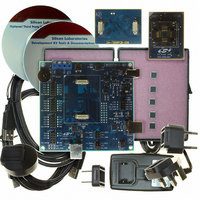
KIT DEV FOR C8051T61X MCU'S
Manufacturer
Silicon Laboratories Inc
Type
MCUr
Specifications of C8051T610DK
Contents
Board, daughter boards, power adapter, cables, documentation and software
Processor To Be Evaluated
C8051T61x
Interface Type
USB
Lead Free Status / RoHS Status
Lead free / RoHS Compliant
For Use With/related Products
C8051T610
For Use With
336-1507 - DAUGHTER BOARD T610 24QFN SOCKET336-1506 - DAUGHTER BOARD T610 28QFN SOCKET336-1505 - DAUGHT BOARD T610 32TQFP SOCKET
Lead Free Status / Rohs Status
Lead free / RoHS Compliant
Other names
336-1443


C8051T610/1/2/3/4/5/6/7
21.2. Assigning Port I/O Pins to Analog and Digital Functions
Port I/O pins can be assigned to various analog, digital, and external interrupt functions. The Port pins
assigned to analog functions should be configured for analog I/O, and Port pins assigned to digital or exter-
nal interrupt functions should be configured for digital I/O.
21.2.1. Assigning Port I/O Pins to Analog Functions
Table 21.1 shows all available analog functions that require Port I/O assignments. Port pins selected for
these analog functions should have their corresponding bit in PnSKIP set to 1. This reserves the pin
for use by the analog function and does not allow it to be claimed by the Crossbar. Table 21.1 shows the
potential mapping of Port I/O to each analog function.
21.2.2. Assigning Port I/O Pins to Digital Functions
Any Port pins not assigned to analog functions may be assigned to digital functions or used as GPIO. Most
digital functions rely on the Crossbar for pin assignment; however, some digital functions bypass the
Crossbar in a manner similar to the analog functions listed above. Port pins used by these digital func-
tions and any Port pins selected for use as GPIO should have their corresponding bit in PnSKIP set
to 1. Table 21.2 shows all available digital functions and the potential mapping of Port I/O to each digital
function.
116
Analog Function
ADC Input
Comparator Inputs
Voltage Reference (VREF0)
External Oscillator in RC or C Mode (EXTCLK)
Digital Function
UART0, SPI0, SMBus, CP0,
CP0A, CP1, CP1A,
SYSCLK, PCA0 (CEX0-4
and ECI), T0 or T1.
Any pin used for GPIO
Table 21.1. Port I/O Assignment for Analog Functions
Table 21.2. Port I/O Assignment for Digital Functions
Any Port pin available for assignment by the
Crossbar. This includes P0.0 - P2.3 pins which
have their PnSKIP bit set to 0.
Note: The Crossbar will always assign UART0
pins to P0.4 and P0.5.
Potentially Assignable Port Pins
Rev 1.0
P0.0–P3.4
Potentially Assignable
P1.0–P3.4
P1.0–P2.7
Port Pins
P0.0
P0.3
CPT0MX, CPT1MX,
OSCXCN, PnSKIP
REF0CN, PnSKIP
SFR(s) used for
SFR(s) used for
AMX0P, PnSKIP
Assignment
XBR0, XBR1
Assignment
PnSKIP
PnSKIP
Related parts for C8051T610DK
Image
Part Number
Description
Manufacturer
Datasheet
Request
R

Part Number:
Description:
SMD/C°/SINGLE-ENDED OUTPUT SILICON OSCILLATOR
Manufacturer:
Silicon Laboratories Inc
Part Number:
Description:
Manufacturer:
Silicon Laboratories Inc
Datasheet:
Part Number:
Description:
N/A N/A/SI4010 AES KEYFOB DEMO WITH LCD RX
Manufacturer:
Silicon Laboratories Inc
Datasheet:
Part Number:
Description:
N/A N/A/SI4010 SIMPLIFIED KEY FOB DEMO WITH LED RX
Manufacturer:
Silicon Laboratories Inc
Datasheet:
Part Number:
Description:
N/A/-40 TO 85 OC/EZLINK MODULE; F930/4432 HIGH BAND (REV E/B1)
Manufacturer:
Silicon Laboratories Inc
Part Number:
Description:
EZLink Module; F930/4432 Low Band (rev e/B1)
Manufacturer:
Silicon Laboratories Inc
Part Number:
Description:
I°/4460 10 DBM RADIO TEST CARD 434 MHZ
Manufacturer:
Silicon Laboratories Inc
Part Number:
Description:
I°/4461 14 DBM RADIO TEST CARD 868 MHZ
Manufacturer:
Silicon Laboratories Inc
Part Number:
Description:
I°/4463 20 DBM RFSWITCH RADIO TEST CARD 460 MHZ
Manufacturer:
Silicon Laboratories Inc
Part Number:
Description:
I°/4463 20 DBM RADIO TEST CARD 868 MHZ
Manufacturer:
Silicon Laboratories Inc
Part Number:
Description:
I°/4463 27 DBM RADIO TEST CARD 868 MHZ
Manufacturer:
Silicon Laboratories Inc
Part Number:
Description:
I°/4463 SKYWORKS 30 DBM RADIO TEST CARD 915 MHZ
Manufacturer:
Silicon Laboratories Inc
Part Number:
Description:
N/A N/A/-40 TO 85 OC/4463 RFMD 30 DBM RADIO TEST CARD 915 MHZ
Manufacturer:
Silicon Laboratories Inc
Part Number:
Description:
I°/4463 20 DBM RADIO TEST CARD 169 MHZ
Manufacturer:
Silicon Laboratories Inc