C8051T610DK Silicon Laboratories Inc, C8051T610DK Datasheet - Page 45
C8051T610DK
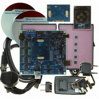
Manufacturer Part Number
C8051T610DK
Description
KIT DEV FOR C8051T61X MCU'S
Manufacturer
Silicon Laboratories Inc
Type
MCUr
Specifications of C8051T610DK
Contents
Board, daughter boards, power adapter, cables, documentation and software
Processor To Be Evaluated
C8051T61x
Interface Type
USB
Lead Free Status / RoHS Status
Lead free / RoHS Compliant
For Use With/related Products
C8051T610
For Use With
336-1507 - DAUGHTER BOARD T610 24QFN SOCKET336-1506 - DAUGHTER BOARD T610 28QFN SOCKET336-1505 - DAUGHT BOARD T610 32TQFP SOCKET
Lead Free Status / Rohs Status
Lead free / RoHS Compliant
Other names
336-1443


SFR Definition 8.4. ADC0CN: ADC0 Control
SFR Address = 0xE8; Bit-Addressable
Name
Reset
Bit
2:0 AD0CM[2:0] ADC0 Start of Conversion Mode Select.
Type
7
6
5
4
3
Bit
AD0BUSY ADC0 Busy Bit.
AD0WINT
AD0INT
AD0EN
AD0TM
Name
AD0EN
R/W
7
0
ADC0 Enable Bit.
0: ADC0 Disabled. ADC0 is in low-power shutdown.
1: ADC0 Enabled. ADC0 is active and ready for data conversions.
ADC0 Track Mode Bit.
0: Normal Track Mode: When ADC0 is enabled, tracking is continuous unless a con-
version is in progress. Conversion begins immediately on start-of-conversion event,
as defined by AD0CM[2:0].
1: Delayed Track Mode: When ADC0 is enabled, input is tracked when a conversion
is not in progress. A start-of-conversion signal initiates three SAR clocks of additional
tracking, and then begins the conversion.
ADC0 Conversion Complete Interrupt Flag.
0: ADC0 has not completed a data conversion since AD0INT was last cleared.
1: ADC0 has completed a data conversion.
ADC0 Window Compare Interrupt Flag.
0: ADC0 Window Comparison Data match has not occurred since this flag was last
cleared.
1: ADC0 Window Comparison Data match has occurred.
000: ADC0 start-of-conversion source is write of 1 to AD0BUSY.
001: ADC0 start-of-conversion source is overflow of Timer 0.
010: ADC0 start-of-conversion source is overflow of Timer 2.
011: ADC0 start-of-conversion source is overflow of Timer 1.
100: ADC0 start-of-conversion source is rising edge of external CNVSTR.
101: ADC0 start-of-conversion source is overflow of Timer 3.
11x: Reserved.
AD0TM
R/W
6
0
AD0INT
R/W
5
0
Read:
0: ADC0 conversion is not in
progress.
1: ADC0 conversion is in prog-
ress.
AD0BUSY AD0WINT
R/W
Rev 1.0
4
0
C8051T610/1/2/3/4/5/6/7
Function
R/W
3
0
Write:
0: No Effect.
1: Initiates ADC0 Conversion if
AD0CM[2:0] = 000b
2
0
AD0CM[2:0]
R/W
1
0
0
0
45
Related parts for C8051T610DK
Image
Part Number
Description
Manufacturer
Datasheet
Request
R

Part Number:
Description:
SMD/C°/SINGLE-ENDED OUTPUT SILICON OSCILLATOR
Manufacturer:
Silicon Laboratories Inc
Part Number:
Description:
Manufacturer:
Silicon Laboratories Inc
Datasheet:
Part Number:
Description:
N/A N/A/SI4010 AES KEYFOB DEMO WITH LCD RX
Manufacturer:
Silicon Laboratories Inc
Datasheet:
Part Number:
Description:
N/A N/A/SI4010 SIMPLIFIED KEY FOB DEMO WITH LED RX
Manufacturer:
Silicon Laboratories Inc
Datasheet:
Part Number:
Description:
N/A/-40 TO 85 OC/EZLINK MODULE; F930/4432 HIGH BAND (REV E/B1)
Manufacturer:
Silicon Laboratories Inc
Part Number:
Description:
EZLink Module; F930/4432 Low Band (rev e/B1)
Manufacturer:
Silicon Laboratories Inc
Part Number:
Description:
I°/4460 10 DBM RADIO TEST CARD 434 MHZ
Manufacturer:
Silicon Laboratories Inc
Part Number:
Description:
I°/4461 14 DBM RADIO TEST CARD 868 MHZ
Manufacturer:
Silicon Laboratories Inc
Part Number:
Description:
I°/4463 20 DBM RFSWITCH RADIO TEST CARD 460 MHZ
Manufacturer:
Silicon Laboratories Inc
Part Number:
Description:
I°/4463 20 DBM RADIO TEST CARD 868 MHZ
Manufacturer:
Silicon Laboratories Inc
Part Number:
Description:
I°/4463 27 DBM RADIO TEST CARD 868 MHZ
Manufacturer:
Silicon Laboratories Inc
Part Number:
Description:
I°/4463 SKYWORKS 30 DBM RADIO TEST CARD 915 MHZ
Manufacturer:
Silicon Laboratories Inc
Part Number:
Description:
N/A N/A/-40 TO 85 OC/4463 RFMD 30 DBM RADIO TEST CARD 915 MHZ
Manufacturer:
Silicon Laboratories Inc
Part Number:
Description:
I°/4463 20 DBM RADIO TEST CARD 169 MHZ
Manufacturer:
Silicon Laboratories Inc