MC56F8367EVME Freescale Semiconductor, MC56F8367EVME Datasheet - Page 120
MC56F8367EVME
Manufacturer Part Number
MC56F8367EVME
Description
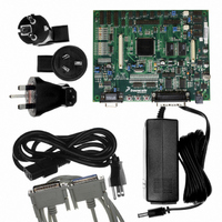
EVAL BOARD FOR MC56F83X
Manufacturer
Freescale Semiconductor
Type
DSPr
Specifications of MC56F8367EVME
Contents
Module and Misc Hardware
Processor To Be Evaluated
MC56F8145-67 and MC56F8345-67
Data Bus Width
16 bit
Interface Type
RS-232
Silicon Manufacturer
Freescale
Core Architecture
56800/E
Core Sub-architecture
56800/E
Silicon Core Number
MC56F
Silicon Family Name
MC56F83xx
Rohs Compliant
Yes
For Use With/related Products
MC56F83x5, MC56F83x6, MC56F83x7
Lead Free Status / RoHS Status
Lead free / RoHS Compliant


6.5.8
Some GPIO pads can have more than one peripheral selected as the alternate function instead of GPIO.
For these pads, this register selects which of the alternate peripherals are actually selected for the GPIO
peripheral function. This applies to GPIOC, pins 0-3, and to GPIOD, pins 0 and 1.
The GPIOC Peripheral Select register can be used to multiplex out any one of the three alternate
peripherals for GPIOC. The default peripheral is Quad Decoder 1 and Quad Timer B (NOT available in
the 56F8167 device); these peripherals work together.
The four I/O pins associated with GPIOC can function as GPIO, Quad Decoder 1/Quad TimerB , or as
SPI 1 signals. GPIO is not the default and is enabled/disabled via the GPIOC_PER, as shown in
Figure 6-10
choice between decoder/timer and SPI inputs/outputs is made in the SIM_GPS register and in conjunction
with the Quad Timer Status and Control Registers (SCR). The default state is for the peripheral function
of GPIOC[3:0] to be programmed as decoder functions. This can be changed by altering the appropriate
controls in the indicated registers.
120
•
•
•
•
•
•
•
•
•
•
•
•
•
•
00100 = Reserved for factory test—PFLASH even clock
00101 = Reserved for factory test—BFLASH clock
00110 = Reserved for factory test—DFLASH clock
00111 = Oscillator output
01000 = F
01001 = Reserved for factory test—IPB clock
01010 = Reserved for factory test—Feedback (from OCCS, this is path to PLL)
01011 = Reserved for factory test—Prescaler clock (from OCCS)
01100 = Reserved for factory test—Postscaler clock (from OCCS)
01101 = Reserved for factory test—SYS_CLK2 (from OCCS)
01110 = Reserved for factory test—SYS_CLK_DIV2
01111 = Reserved for factory test—SYS_CLK_D
10000 = ADCA clock
10001 = ADCB clock
GPIO Peripheral Select Register (SIM_GPS)
and
out
Table
(from OCCS)
6-2. When GPIOC[3:0] are programmed to operate as peripheral I/O, then the
56F8367 Technical Data, Rev. 8
Freescale Semiconductor
Preliminary
Related parts for MC56F8367EVME
Image
Part Number
Description
Manufacturer
Datasheet
Request
R

Part Number:
Description:
56f8300 16-bit Digital Signal Controllers
Manufacturer:
Freescale Semiconductor, Inc
Datasheet:
Part Number:
Description:
Manufacturer:
Freescale Semiconductor, Inc
Datasheet:
Part Number:
Description:
Manufacturer:
Freescale Semiconductor, Inc
Datasheet:
Part Number:
Description:
Manufacturer:
Freescale Semiconductor, Inc
Datasheet:
Part Number:
Description:
Manufacturer:
Freescale Semiconductor, Inc
Datasheet:
Part Number:
Description:
Manufacturer:
Freescale Semiconductor, Inc
Datasheet:
Part Number:
Description:
Manufacturer:
Freescale Semiconductor, Inc
Datasheet:
Part Number:
Description:
Manufacturer:
Freescale Semiconductor, Inc
Datasheet:
Part Number:
Description:
Manufacturer:
Freescale Semiconductor, Inc
Datasheet:
Part Number:
Description:
Manufacturer:
Freescale Semiconductor, Inc
Datasheet:
Part Number:
Description:
Manufacturer:
Freescale Semiconductor, Inc
Datasheet:
Part Number:
Description:
Manufacturer:
Freescale Semiconductor, Inc
Datasheet:
Part Number:
Description:
Manufacturer:
Freescale Semiconductor, Inc
Datasheet:
Part Number:
Description:
Manufacturer:
Freescale Semiconductor, Inc
Datasheet:
Part Number:
Description:
Manufacturer:
Freescale Semiconductor, Inc
Datasheet: