MC56F8367EVME Freescale Semiconductor, MC56F8367EVME Datasheet - Page 123
MC56F8367EVME
Manufacturer Part Number
MC56F8367EVME
Description
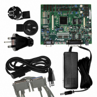
EVAL BOARD FOR MC56F83X
Manufacturer
Freescale Semiconductor
Type
DSPr
Specifications of MC56F8367EVME
Contents
Module and Misc Hardware
Processor To Be Evaluated
MC56F8145-67 and MC56F8345-67
Data Bus Width
16 bit
Interface Type
RS-232
Silicon Manufacturer
Freescale
Core Architecture
56800/E
Core Sub-architecture
56800/E
Silicon Core Number
MC56F
Silicon Family Name
MC56F83xx
Rohs Compliant
Yes
For Use With/related Products
MC56F83x5, MC56F83x6, MC56F83x7
Lead Free Status / RoHS Status
Lead free / RoHS Compliant


6.5.8.2
This bit selects the alternate function for GPIOD1.
6.5.8.3
6.5.8.4
This bit selects the alternate function for GPIOC3.
6.5.8.5
This bit selects the alternate function for GPIOC2.
6.5.8.6
This bit selects the alternate function for GPIOC1.
6.5.8.7
This bit selects the alternate function for GPIOC0.
6.5.9
The Peripheral Clock Enable register is used enable or disable clocks to the peripherals as a power savings
feature. The clocks can be individually controlled for each peripheral on the chip.
Freescale Semiconductor
Preliminary
•
•
•
•
•
•
•
•
•
•
•
•
Base + $C
RESET
Read
Write
0 = CS3
1 = CAN2_RX
0 = CS2
1 = CAN2_TX
0 = HOME1/TB3 (default - see “Switch Matrix Mode” bits of the Quad Decoder DECCR register in the
56F8300 Peripheral User Manual)
1 = SS1
0 = INDEX1/TB2 (default)
1 = MISO1
0 = PHASEB1/TB1 (default)
1 = MOSI1
0 = PHASEA1/TB0 (default)
1 = SCLK1
Peripheral Clock Enable Register (SIM_PCE)
GPIOD1 (D1)—Bit 5
GPIOD0 (D0)—Bit 4
GPIOC3 (C3)—Bit 3
GPIOC2 (C2)—Bit 2
GPIOC1 (C1)—Bit 1
GPIOC0 (C0)—Bit 0
EMI
15
1
Figure 6-13 Peripheral Clock Enable Register (SIM_PCE)
ADCB ADCA CAN DEC1 DEC0 TMRD TMRC
14
1
13
1
12
1
11
1
56F8367 Technical Data, Rev. 8
10
1
9
1
8
1
TMRB TMRA SCI 1 SCI 0
7
1
6
1
5
1
4
1
SPI 1
3
1
SPI 0
2
1
Register Descriptions
PWMB
1
1
PWMA
0
1
123
Related parts for MC56F8367EVME
Image
Part Number
Description
Manufacturer
Datasheet
Request
R

Part Number:
Description:
56f8300 16-bit Digital Signal Controllers
Manufacturer:
Freescale Semiconductor, Inc
Datasheet:
Part Number:
Description:
Manufacturer:
Freescale Semiconductor, Inc
Datasheet:
Part Number:
Description:
Manufacturer:
Freescale Semiconductor, Inc
Datasheet:
Part Number:
Description:
Manufacturer:
Freescale Semiconductor, Inc
Datasheet:
Part Number:
Description:
Manufacturer:
Freescale Semiconductor, Inc
Datasheet:
Part Number:
Description:
Manufacturer:
Freescale Semiconductor, Inc
Datasheet:
Part Number:
Description:
Manufacturer:
Freescale Semiconductor, Inc
Datasheet:
Part Number:
Description:
Manufacturer:
Freescale Semiconductor, Inc
Datasheet:
Part Number:
Description:
Manufacturer:
Freescale Semiconductor, Inc
Datasheet:
Part Number:
Description:
Manufacturer:
Freescale Semiconductor, Inc
Datasheet:
Part Number:
Description:
Manufacturer:
Freescale Semiconductor, Inc
Datasheet:
Part Number:
Description:
Manufacturer:
Freescale Semiconductor, Inc
Datasheet:
Part Number:
Description:
Manufacturer:
Freescale Semiconductor, Inc
Datasheet:
Part Number:
Description:
Manufacturer:
Freescale Semiconductor, Inc
Datasheet:
Part Number:
Description:
Manufacturer:
Freescale Semiconductor, Inc
Datasheet: