MC56F8367EVME Freescale Semiconductor, MC56F8367EVME Datasheet - Page 19
MC56F8367EVME
Manufacturer Part Number
MC56F8367EVME
Description
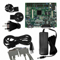
EVAL BOARD FOR MC56F83X
Manufacturer
Freescale Semiconductor
Type
DSPr
Specifications of MC56F8367EVME
Contents
Module and Misc Hardware
Processor To Be Evaluated
MC56F8145-67 and MC56F8345-67
Data Bus Width
16 bit
Interface Type
RS-232
Silicon Manufacturer
Freescale
Core Architecture
56800/E
Core Sub-architecture
56800/E
Silicon Core Number
MC56F
Silicon Family Name
MC56F83xx
Rohs Compliant
Yes
For Use With/related Products
MC56F83x5, MC56F83x6, MC56F83x7
Lead Free Status / RoHS Status
Lead free / RoHS Compliant


Freescale Semiconductor
Preliminary
* When the on-chip regulator is disabled, these four pins become 2.5V V
Table 2-2 Signal and Package Information for the 160-Pin LQFP and MBGA (Continued)
CLKMODE
V
OCR_DIS
V
V
V
V
EXTAL
SSA_ADC
Signal
Name
V
V
CAP
CAP
CAP
CAP
V
V
V
V
V
V
PP
PP
SS
SS
SS
SS
SS
SS
1
2
1*
2*
3*
4*
No.
125
160
115
144
141
Pin
27
41
74
80
91
62
95
15
99
94
2
Ball No.
G11
D12
H11
H12
K11
K14
J11
J12
G4
C2
E7
E6
K8
E8
A7
J4
Supply
Supply
Supply
Type
Input
Input
Input
Input
56F8367 Technical Data, Rev. 8
During
Supply
Reset
State
Input
Input
Input
Input
V
ADC Analog Ground — This pin supplies an analog ground to
the ADC modules.
On-Chip Regulator Disable —
Tie this pin to V
Tie this pin to V
This pin is intended to be a static DC signal from power-up to
shut down. Do not try to toggle this pin for power savings
during operation.
V
connect each pin to a 2.2μF or greater bypass capacitor in order
to bypass the core logic voltage regulator, required for proper chip
operation. When OCR_DIS is tied to V
these pins become V
regulated 2.5V power supply.
Note: This bypass is required even if the chip is powered
with an external supply.
V
circuit for normal functionality.
Clock Input Mode Selection — This input determines the
function of the XTAL and EXTAL pins.
1 = External clock input on XTAL is used to directly drive the input
clock of the chip. The EXTAL pin should be grounded.
0 = A crystal or ceramic resonator should be connected between
XTAL and EXTAL.
External Crystal Oscillator Input — This input can be
connected to an 8MHz external crystal. Tie this pin low if XTAL is
driven by an external clock source.
SS
CAP
PP
1 - 2 — These pins should be left unconnected as an open
— These pins provide ground for chip logic and I/O drivers.
1 - 4 — When OCR_DIS is tied to V
DD_CORE
SS
DD
to enable the on-chip regulator
to disable the on-chip regulator
DD_CORE
.
Signal Description
and should be connected to a
DD
SS
(regulator disabled),
(regulator enabled),
Signal Pins
19
Related parts for MC56F8367EVME
Image
Part Number
Description
Manufacturer
Datasheet
Request
R

Part Number:
Description:
56f8300 16-bit Digital Signal Controllers
Manufacturer:
Freescale Semiconductor, Inc
Datasheet:
Part Number:
Description:
Manufacturer:
Freescale Semiconductor, Inc
Datasheet:
Part Number:
Description:
Manufacturer:
Freescale Semiconductor, Inc
Datasheet:
Part Number:
Description:
Manufacturer:
Freescale Semiconductor, Inc
Datasheet:
Part Number:
Description:
Manufacturer:
Freescale Semiconductor, Inc
Datasheet:
Part Number:
Description:
Manufacturer:
Freescale Semiconductor, Inc
Datasheet:
Part Number:
Description:
Manufacturer:
Freescale Semiconductor, Inc
Datasheet:
Part Number:
Description:
Manufacturer:
Freescale Semiconductor, Inc
Datasheet:
Part Number:
Description:
Manufacturer:
Freescale Semiconductor, Inc
Datasheet:
Part Number:
Description:
Manufacturer:
Freescale Semiconductor, Inc
Datasheet:
Part Number:
Description:
Manufacturer:
Freescale Semiconductor, Inc
Datasheet:
Part Number:
Description:
Manufacturer:
Freescale Semiconductor, Inc
Datasheet:
Part Number:
Description:
Manufacturer:
Freescale Semiconductor, Inc
Datasheet:
Part Number:
Description:
Manufacturer:
Freescale Semiconductor, Inc
Datasheet:
Part Number:
Description:
Manufacturer:
Freescale Semiconductor, Inc
Datasheet: