MC56F8367EVME Freescale Semiconductor, MC56F8367EVME Datasheet - Page 21
MC56F8367EVME
Manufacturer Part Number
MC56F8367EVME
Description
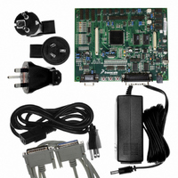
EVAL BOARD FOR MC56F83X
Manufacturer
Freescale Semiconductor
Type
DSPr
Specifications of MC56F8367EVME
Contents
Module and Misc Hardware
Processor To Be Evaluated
MC56F8145-67 and MC56F8345-67
Data Bus Width
16 bit
Interface Type
RS-232
Silicon Manufacturer
Freescale
Core Architecture
56800/E
Core Sub-architecture
56800/E
Silicon Core Number
MC56F
Silicon Family Name
MC56F83xx
Rohs Compliant
Yes
For Use With/related Products
MC56F83x5, MC56F83x6, MC56F83x7
Lead Free Status / RoHS Status
Lead free / RoHS Compliant


Freescale Semiconductor
Preliminary
Table 2-2 Signal and Package Information for the 160-Pin LQFP and MBGA (Continued)
(GPIOE2)
(GPIOE3)
(GPIOA0)
(GPIOA1)
(GPIOA2)
(GPIOA3)
(GPIOA4)
(GPIOA5)
(GPIOA6)
(GPIOA7)
Signal
Name
A10
A11
A12
A13
A14
A15
A6
A7
A8
A9
No.
Pin
17
18
19
20
21
22
23
24
25
26
Ball No.
G1
G3
G2
H1
H2
H4
H3
J1
J2
J3
Schmitt
Schmitt
Output
Output
Output
Output
Input/
Input/
Type
56F8367 Technical Data, Rev. 8
disabled,
pull-up is
disabled,
pull-up is
output is
output is
In reset,
In reset,
enabled
enabled
During
Reset
State
Address Bus — A6 - A7 specify two of the address lines for
external program or data memory accesses.
Depending upon the state of the DRV bit in the EMI bus control
register (BCR), A6 - A7 and EMI control signals are tri-stated when
the external bus is inactive.
Most designs will want to change the DRV state to DRV = 1 instead
of using the default setting.
Port E GPIO — These two GPIO pins can be individually
programmed as input or output pins.
After reset, the default state is Address Bus.
To deactivate the internal pull-up resistor, clear the appropriate
GPIO bit in the GPIOE_PUR register.
Example: GPIOE2, clear bit 2 in the GPIOE_PUR register.
Address Bus— A8 - A15 specify eight of the address lines for
external program or data memory accesses.
Depending upon the state of the DRV bit in the EMI bus control
register (BCR), A8 - A15 and EMI control signals are tri-stated when
the external bus is inactive.
Most designs will want to change the DRV state to DRV = 1 instead
of using the default setting.
Port A GPIO — These eight GPIO pins can be individually
programmed as input or output pins.
After reset, the default state is Address Bus.
To deactivate the internal pull-up resistor, clear the appropriate
GPIO bit in the GPIOA_PUR register.
Example: GPIOA0, clear bit 0 in the GPIOA_PUR register.
Signal Description
Signal Pins
21
Related parts for MC56F8367EVME
Image
Part Number
Description
Manufacturer
Datasheet
Request
R

Part Number:
Description:
56f8300 16-bit Digital Signal Controllers
Manufacturer:
Freescale Semiconductor, Inc
Datasheet:
Part Number:
Description:
Manufacturer:
Freescale Semiconductor, Inc
Datasheet:
Part Number:
Description:
Manufacturer:
Freescale Semiconductor, Inc
Datasheet:
Part Number:
Description:
Manufacturer:
Freescale Semiconductor, Inc
Datasheet:
Part Number:
Description:
Manufacturer:
Freescale Semiconductor, Inc
Datasheet:
Part Number:
Description:
Manufacturer:
Freescale Semiconductor, Inc
Datasheet:
Part Number:
Description:
Manufacturer:
Freescale Semiconductor, Inc
Datasheet:
Part Number:
Description:
Manufacturer:
Freescale Semiconductor, Inc
Datasheet:
Part Number:
Description:
Manufacturer:
Freescale Semiconductor, Inc
Datasheet:
Part Number:
Description:
Manufacturer:
Freescale Semiconductor, Inc
Datasheet:
Part Number:
Description:
Manufacturer:
Freescale Semiconductor, Inc
Datasheet:
Part Number:
Description:
Manufacturer:
Freescale Semiconductor, Inc
Datasheet:
Part Number:
Description:
Manufacturer:
Freescale Semiconductor, Inc
Datasheet:
Part Number:
Description:
Manufacturer:
Freescale Semiconductor, Inc
Datasheet:
Part Number:
Description:
Manufacturer:
Freescale Semiconductor, Inc
Datasheet: