MPC566EVB Freescale Semiconductor, MPC566EVB Datasheet - Page 18
MPC566EVB
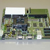
Manufacturer Part Number
MPC566EVB
Description
KIT EVALUATION FOR MPC565/566
Manufacturer
Freescale Semiconductor
Specifications of MPC566EVB
Processor To Be Evaluated
MPC56x
Data Bus Width
32 bit
Interface Type
RS-232, Ethernet
Lead Free Status / RoHS Status
Contains lead / RoHS non-compliant


Freescale Semiconductor, Inc.
Support Logic
ROM to start at 0x0080_0000 and configures the rest of the internal and external peripherals.
Please refer to the MPC565 user’s manual (Global (Boot) Chip-Select Operation) for more
information.
1.3 Support Logic
1.3.1 Reset Logic
The reset logic provides system initialization. Reset occurs during power-on or via assertion of the
signal RESET which causes the MPC566 to reset. HRESET is triggered by the reset switch (SW1)
which resets the entire processor/system.
dBUG configures the MPC566 microprocessor internal resources during initialization. The
contents of the exception table are copied to address 0xFFF0_0000 in the SDRAM. The Software
Watchdog Timer is disabled, the Bus Monitor is enabled, and the internal timers are placed in a stop
condition. A memory map for the entire board can be seen in Table 1-1., “The MPC566EVB
Default Memory Map”.
RW0 – 30: External Reset Configuration Word (RCW) Options
RW0, RW2, RW4 – 18, RW23 – 30 provide the user access to external Reset Configuration Word
(RCW) bits not normally required for default MPC566EVB operation. The RW0 – 30 designations
reflect the data bus D0 – D30 bit effected when the RCW word is enabled externally. All RW0 –
30 option bits are defaulted to the logic low value during external RCW word operation. The user
may apply a wire jumper between the 2 pad positions of each RW0 – 30 option to provide a logic
high level on the respective bit position during external RCW operation. Refer to the MPC566 user
manual Reset chapter for the respective RCW bit definitions.
1.3.2 Clock Circuitry
The MPC566EVB board uses a 4MHz crystal (Y1 on the schematics) to provide the clock to the
on-chip oscillator of the MPC566. In addition to the 4MHz crystal, there is also a 25MHz oscillator
(Y3) which feeds the Ethernet chip (U20).
1.3.3 Watchdog Timer
The duration of the Watchdog is selected by the SWT[1:0] bits in the System Protection and
28
Control Register (SYPCR), SWT[1:0] = 0b11 gives a maximum timeout period of 2
/System
frequency. The dBUG monitor initializes these bits with the value 0b11, which provides the
maximum time-out period, but dBUG does NOT enable the watchdog timer via the SYPCR
register SWE bit.
1.3.4 Exception Sources
The MPC500 family of processors can receive exceptions as a result of external signals, errors,
interrupts, or unusual conditions arising in the execution of instructions. When the processor
receives an exception, information about the state of the processor is saved and, after switching to
supervisor mode, the processor begins handling the exception based on instructions in the
1-8
MPC566EVB User’s Manual
For More Information On This Product,
Go to: www.freescale.com
Related parts for MPC566EVB
Image
Part Number
Description
Manufacturer
Datasheet
Request
R

Part Number:
Description:
Manufacturer:
Freescale Semiconductor, Inc
Datasheet:
Part Number:
Description:
Manufacturer:
Freescale Semiconductor, Inc
Datasheet:
Part Number:
Description:
Manufacturer:
Freescale Semiconductor, Inc
Datasheet:
Part Number:
Description:
Manufacturer:
Freescale Semiconductor, Inc
Datasheet:
Part Number:
Description:
Manufacturer:
Freescale Semiconductor, Inc
Datasheet:
Part Number:
Description:
Manufacturer:
Freescale Semiconductor, Inc
Datasheet:
Part Number:
Description:
Manufacturer:
Freescale Semiconductor, Inc
Datasheet:
Part Number:
Description:
Manufacturer:
Freescale Semiconductor, Inc
Datasheet:
Part Number:
Description:
Manufacturer:
Freescale Semiconductor, Inc
Datasheet:
Part Number:
Description:
Manufacturer:
Freescale Semiconductor, Inc
Datasheet:
Part Number:
Description:
Manufacturer:
Freescale Semiconductor, Inc
Datasheet:
Part Number:
Description:
Manufacturer:
Freescale Semiconductor, Inc
Datasheet:
Part Number:
Description:
Manufacturer:
Freescale Semiconductor, Inc
Datasheet:
Part Number:
Description:
Manufacturer:
Freescale Semiconductor, Inc
Datasheet:
Part Number:
Description:
Manufacturer:
Freescale Semiconductor, Inc
Datasheet: