MPC566EVB Freescale Semiconductor, MPC566EVB Datasheet - Page 26
MPC566EVB
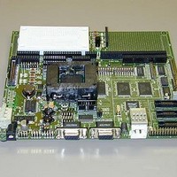
Manufacturer Part Number
MPC566EVB
Description
KIT EVALUATION FOR MPC565/566
Manufacturer
Freescale Semiconductor
Specifications of MPC566EVB
Processor To Be Evaluated
MPC56x
Data Bus Width
32 bit
Interface Type
RS-232, Ethernet
Lead Free Status / RoHS Status
Contains lead / RoHS non-compliant


Communication Ports
The signals which are neccessary for debug are available at connector (BDM_PORT). Figure 1-3
shows the (BDM_PORT) Connector pin assignment.
V1, V2, V3, and V4
The V1 – V4 options provide a way to use the alternate VFLS0 and VFLS1 BDM signals from the
MPC566. By default, the primary VFLS0 and VFLS1 signals are applied by V1 and V2 default
connections. To modify the BDM port to apply the alternate VFLS0 and VFLS1 signals, options
V1 and V2 should be cut and options V3 and V4 connected.
1.4.4.2 Nexus Connector
The 2001-Nexus standard defines several different standards for different speed accesses to a
microcontroller in a target system. These standards have been revised since that release. The new
connectors come in both a robust and a non-robust configuration. In addition, each connector has
2 definitions depending upon whether the connection is an Auxiliary only (Auxiliary In and
Auxiliary Out) connection or a JTAG IEEE 1149.1 port with an Auxiliary Output port.
1-16
JP3
2.6 or 3.3 V
The MPC56x parts do not support the JTAG IEEE 1149.1 configuration.
Figure 1-3. The BDM_PORT Connector pin assignment
3.3V
2.6V
HRESET
VFLS0
Power
GND
GND
Freescale Semiconductor, Inc.
For More Information On This Product,
MPC566EVB User’s Manual
Go to: www.freescale.com
1
3
5
7
9
NOTE
10
2
4
6
8
SRESET
DSCK
VFLS1
DSDI
DSO
Related parts for MPC566EVB
Image
Part Number
Description
Manufacturer
Datasheet
Request
R

Part Number:
Description:
Manufacturer:
Freescale Semiconductor, Inc
Datasheet:
Part Number:
Description:
Manufacturer:
Freescale Semiconductor, Inc
Datasheet:
Part Number:
Description:
Manufacturer:
Freescale Semiconductor, Inc
Datasheet:
Part Number:
Description:
Manufacturer:
Freescale Semiconductor, Inc
Datasheet:
Part Number:
Description:
Manufacturer:
Freescale Semiconductor, Inc
Datasheet:
Part Number:
Description:
Manufacturer:
Freescale Semiconductor, Inc
Datasheet:
Part Number:
Description:
Manufacturer:
Freescale Semiconductor, Inc
Datasheet:
Part Number:
Description:
Manufacturer:
Freescale Semiconductor, Inc
Datasheet:
Part Number:
Description:
Manufacturer:
Freescale Semiconductor, Inc
Datasheet:
Part Number:
Description:
Manufacturer:
Freescale Semiconductor, Inc
Datasheet:
Part Number:
Description:
Manufacturer:
Freescale Semiconductor, Inc
Datasheet:
Part Number:
Description:
Manufacturer:
Freescale Semiconductor, Inc
Datasheet:
Part Number:
Description:
Manufacturer:
Freescale Semiconductor, Inc
Datasheet:
Part Number:
Description:
Manufacturer:
Freescale Semiconductor, Inc
Datasheet:
Part Number:
Description:
Manufacturer:
Freescale Semiconductor, Inc
Datasheet: