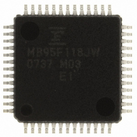
MB95F118JWPMC-GE1 Fujitsu Semiconductor America Inc, MB95F118JWPMC-GE1 Datasheet - Page 14

MB95F118JWPMC-GE1
Manufacturer Part Number
MB95F118JWPMC-GE1
Description
IC MCU 60K FLASH 2KB RAM 52LQFP
Manufacturer
Fujitsu Semiconductor America Inc
Series
F²MC MB95110Mr
Datasheet
1.MB95F118JWPMC-GE1.pdf
(76 pages)
Specifications of MB95F118JWPMC-GE1
Core Processor
F²MC-8FX
Core Size
8-Bit
Speed
16MHz
Connectivity
I²C, LIN, SIO, UART/USART
Peripherals
LVD, POR, PWM, WDT
Number Of I /o
39
Program Memory Size
60KB (60K x 8)
Program Memory Type
FLASH
Ram Size
2K x 8
Voltage - Supply (vcc/vdd)
2.4 V ~ 5.5 V
Data Converters
A/D 8x8/10b
Oscillator Type
External
Operating Temperature
-40°C ~ 85°C
Package / Case
52-LQFP
Lead Free Status / RoHS Status
Lead free / RoHS Compliant
Eeprom Size
-
Other names
865-1071
Available stocks
Company
Part Number
Manufacturer
Quantity
Price
Company:
Part Number:
MB95F118JWPMC-GE1
Manufacturer:
AD
Quantity:
1 000
Company:
Part Number:
MB95F118JWPMC-GE1
Manufacturer:
Fujitsu Semiconductor America Inc
Quantity:
10 000
14
MB95110M Series
■ HANDLING DEVICES
• Preventing Latch-up
• Stable Supply Voltage
• Precautions for Use of External Clock
PIN CONNECTION
• Treatment of Unused Pin
• Treatment of Power Supply Pins on A/D Converter
• Power Supply Pins
Care must be taken to ensure that maximum voltage ratings are not exceeded when they are used.
Latch-up may occur on CMOS ICs if voltage higher than V
other than medium- and high-withstand voltage pins or if higher than the rating voltage is applied between V
pin and V
When latch-up occurs, power supply current increases rapidly and might thermally damage elements.
Also, take care to prevent the analog power supply voltage (AV
digital power supply voltage (V
Supply voltage should be stabilized.
A sudden change in power-supply voltage may cause a malfunction even within the guaranteed operating range
of the Vcc power-supply voltage.
For stabilization, in principle, keep the variation in Vcc ripple (p-p value) in a commercial frequency range
(50/60 Hz) not to exceed 10% of the standard Vcc value and suppress the voltage variation so that the transient
variation rate does not exceed 0.1 V/ms during a momentary change such as when the power supply is switched.
Even when an external clock is used, oscillation stabilization wait time is required for power-on reset, wake-up
from sub clock mode or stop mode.
Leaving unused input pins unconnected can cause abnormal operation or latch-up, leaving to permanent damage.
Unused input pins should always be pulled up or down through resistance of at least 2 kΩ. Any unused input/
output pins may be set to output mode and left open, or set to input mode and treated the same as unused input
pins. If there is unused output pin, make it open.
Connect to be AV
Noise riding on the AV
as a bypass capacitor between AV
In products with multiple V
to avoid abnormal operations including latch-up. However, you must connect the pins to external power supply
and a ground line to lower the electro-magnetic emission level, to prevent abnormal operation of strobe signals
caused by the rise in the ground level, and to conform to the total output current rating.
Moreover, connect the current supply source with the V
It is also advisable to connect a ceramic bypass capacitor of approximately 0.1 µF between V
near this device.
SS
pin.
CC
= V
CC
CC
pin may cause accuracy degradation. So, connect approx. 0.1 µF ceramic capacitor
and AV
CC
or V
CC
) when the analog system power supply is turned on or off.
SS
SS
CC
= V
pins, the pins of the same potential are internally connected in the device
and AV
SS
even if the A/D converter is not in use.
SS
pins in the vicinity of this device.
CC
CC
and V
or lower than V
CC
SS
) and analog input voltage from exceeding the
pins of this device at the low impedance.
SS
is applied to input and output pins
CC
and V
SS
pins
CC


