MB95F118JWPMC-GE1 Fujitsu Semiconductor America Inc, MB95F118JWPMC-GE1 Datasheet - Page 72
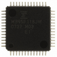
MB95F118JWPMC-GE1
Manufacturer Part Number
MB95F118JWPMC-GE1
Description
IC MCU 60K FLASH 2KB RAM 52LQFP
Manufacturer
Fujitsu Semiconductor America Inc
Series
F²MC MB95110Mr
Datasheet
1.MB95F118JWPMC-GE1.pdf
(76 pages)
Specifications of MB95F118JWPMC-GE1
Core Processor
F²MC-8FX
Core Size
8-Bit
Speed
16MHz
Connectivity
I²C, LIN, SIO, UART/USART
Peripherals
LVD, POR, PWM, WDT
Number Of I /o
39
Program Memory Size
60KB (60K x 8)
Program Memory Type
FLASH
Ram Size
2K x 8
Voltage - Supply (vcc/vdd)
2.4 V ~ 5.5 V
Data Converters
A/D 8x8/10b
Oscillator Type
External
Operating Temperature
-40°C ~ 85°C
Package / Case
52-LQFP
Lead Free Status / RoHS Status
Lead free / RoHS Compliant
Eeprom Size
-
Other names
865-1071
Available stocks
Company
Part Number
Manufacturer
Quantity
Price
Company:

Part Number:
MB95F118JWPMC-GE1
Manufacturer:
AD
Quantity:
1 000
Company:
Part Number:
MB95F118JWPMC-GE1
Manufacturer:
Fujitsu Semiconductor America Inc
Quantity:
10 000


72
MB95110M Series
■ MAIN CHANGES IN THIS EDITION
The vertical lines marked in the left side of the page show the changes.
62 to 67
Page
11
24
37
39
41
⎯
2
4
6
7
■
■
■
■
• Difference between RST and MOD Pins
■
■
■
4. AC Characteristics
(1) Clock Timing
(2) Source Clock/Machine Clock
■
FEATURES
PRODUCT LINEUP
I/O CIRCUIT TYPE
I/O MAP
ELECTRICAL CHARACTERISTICS
EXAMPLE CHARACTERISTICS
PACKAGES AND CORRESPONDING
PRODUCTS
DIFFERENCES AMONG PRODUCTS
AND NOTES ON SELECTING
PRODUCTS
Section
⎯
No third edition in the DS07-12611-4E.
Added the description Dual operation Flash memory.
Changed the contents of Option.
Changed FPT-52P-M01 of MB95117M as follows;
* (Under development) →
Deleted as follows;
“The input type of RST and MOD pins is CMOS inputs on
the Flash memory product. The RST and MOD pins are
hysteresis inputs on the MASK ROM product.”
Changed as follows in the remarks of “Type B”.
Hysteresis input only for MASK ROM product →
Hysteresis input
Changed as follows for R/W of Reset source register
R → R/W
Added “Main PLL multiplied by 4” in the Clock frequency
• Changed in the remarks of source clock cycle time
(when using main clock)
Min : F
→ Min : F
• Changed the footnote of *1;
PLL multiplication of main clock (select from 1, 2, 2.5 mul-
tiplication) → PLL multiplication of main clock (select
from 1, 2, 2.5,4 multiplication)
• Added “ × 4” in the Main PLL of “• Outline of clock
generation block”
Changed the figure of • Main PLL operation frequency
Added the
CH
= 16.25 MHz, PLL multiplied by 1
CH
■
= 8.125 MHz, PLL multiplied by 2
EXAMPLE CHARACTERISTICS
Change Results
(Available).
Related parts for MB95F118JWPMC-GE1
Image
Part Number
Description
Manufacturer
Datasheet
Request
R

Part Number:
Description:
IC POWER SUPPLY MONITOR 8SOP
Manufacturer:
Fujitsu Semiconductor America Inc
Datasheet:
Part Number:
Description:
IC POWER SUPPLY MONITOR 8SOP
Manufacturer:
Fujitsu Semiconductor America Inc
Datasheet:

Part Number:
Description:
IC MCU 32BIT 256KB FLASH 120LQFP
Manufacturer:
Fujitsu Semiconductor America Inc
Datasheet:
Part Number:
Description:
IC CTLR TOUCH SENSOR 12CH 30SSOP
Manufacturer:
Fujitsu Semiconductor America Inc
Datasheet:

Part Number:
Description:
IC CTLR TOUCH SENSOR 12CH 40QFN
Manufacturer:
Fujitsu Semiconductor America Inc
Datasheet:
Part Number:
Description:
SYNTHESIZER PLL DUAL INP 20SSOP
Manufacturer:
Fujitsu Semiconductor America Inc
Datasheet:

Part Number:
Description:
SYNTHESZR PLL 1.1GHZ DUAL 16SSOP
Manufacturer:
Fujitsu Semiconductor America Inc
Datasheet:

Part Number:
Description:
IC SSCG EMI RED 8-SOIC
Manufacturer:
Fujitsu Semiconductor America Inc
Datasheet:

Part Number:
Description:
IC SSCG EMI RED 8-TSSOP
Manufacturer:
Fujitsu Semiconductor America Inc
Datasheet:

Part Number:
Description:
IC SSCG EMI RED 8-SOP
Manufacturer:
Fujitsu Semiconductor America Inc
Datasheet:

Part Number:
Description:
SYNTHESIZER PLL 2.5GHZ 16SSOP
Manufacturer:
Fujitsu Semiconductor America Inc
Datasheet:
Part Number:
Description:
SYNTHESIZER PLL 1.2GHZ 16SSOP
Manufacturer:
Fujitsu Semiconductor America Inc
Datasheet:

Part Number:
Description:
SYNTHESIZER PLL 2.5GHZ 16BCC
Manufacturer:
Fujitsu Semiconductor America Inc
Datasheet:

Part Number:
Description:
IC SSCG EMI RED 8-SOP
Manufacturer:
Fujitsu Semiconductor America Inc
Datasheet:
Part Number:
Description:
IC SSCG EMI RED 16-BCC
Manufacturer:
Fujitsu Semiconductor America Inc
Datasheet: