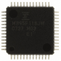
MB95F118JWPMC-GE1 Fujitsu Semiconductor America Inc, MB95F118JWPMC-GE1 Datasheet - Page 22

MB95F118JWPMC-GE1
Manufacturer Part Number
MB95F118JWPMC-GE1
Description
IC MCU 60K FLASH 2KB RAM 52LQFP
Manufacturer
Fujitsu Semiconductor America Inc
Series
F²MC MB95110Mr
Datasheet
1.MB95F118JWPMC-GE1.pdf
(76 pages)
Specifications of MB95F118JWPMC-GE1
Core Processor
F²MC-8FX
Core Size
8-Bit
Speed
16MHz
Connectivity
I²C, LIN, SIO, UART/USART
Peripherals
LVD, POR, PWM, WDT
Number Of I /o
39
Program Memory Size
60KB (60K x 8)
Program Memory Type
FLASH
Ram Size
2K x 8
Voltage - Supply (vcc/vdd)
2.4 V ~ 5.5 V
Data Converters
A/D 8x8/10b
Oscillator Type
External
Operating Temperature
-40°C ~ 85°C
Package / Case
52-LQFP
Lead Free Status / RoHS Status
Lead free / RoHS Compliant
Eeprom Size
-
Other names
865-1071
Available stocks
Company
Part Number
Manufacturer
Quantity
Price
Company:
Part Number:
MB95F118JWPMC-GE1
Manufacturer:
AD
Quantity:
1 000
Company:
Part Number:
MB95F118JWPMC-GE1
Manufacturer:
Fujitsu Semiconductor America Inc
Quantity:
10 000
22
MB95110M Series
• Rule for Conversion of Actual Addresses in the General-purpose Register Area
The RP indicates the address of the register bank currently being used. The relationship between the content
of RP and the real address conforms to the conversion rule illustrated below:
The DP specifies the area for mapping instructions (16 different instructions such as MOV A, dir) using direct
addresses to 0080
The CCR consists of the bits indicating arithmetic operation results or transfer data contents and the bits that
control CPU operations at interrupt.
Direct bank pointer (DP2 to DP0)
N flag
Z flag
V flag
C flag
H flag
I flag
IL1, IL0 : Indicates the level of the interrupt currently enabled. Processes an interrupt only if its request level
Generated address
XXX
IL1
0
0
1
1
B
000
: Set to “1” if the MSB is set to “1” as the result of an arithmetic operation. Cleared to “0” when the
: Set to “1” when an arithmetic operation results in “0”. Cleared to “0” otherwise.
: Set to “1” if the complement on 2 overflows as a result of an arithmetic operation. Cleared to “0”
: Set to “1” when a carry or a borrow from bit 7 occurs as a result of an arithmetic operation. Cleared
(no effect to mapping)
: Set to “1” when a carry or a borrow from bit 3 to bit 4 occurs as a result of an arithmetic operation.
: Interrupt is enabled when this flag is set to “1”. Interrupt is disabled when this flag is set to “0”.
bit is set to “0”.
otherwise.
to “0” otherwise. Set to the shift-out value in the case of a shift instruction.
Cleared to “0” otherwise. This flag is for decimal adjustment instructions.
The flag is set to “0” when reset.
is higher than the value indicated by these bits.
B
(initial value)
001
010
011
100
101
110
111
H
B
B
B
B
B
B
B
to 00FF
A15 A14 A13 A12 A11 A10
"0"
IL0
0
1
0
1
H
.
"0"
"0"
"0"
Specified address area
"0"
0000
0080
Interrupt level
"0"
H
H
"0"
A9
to 007F
to 00FF
0
1
2
3
"1"
A8
H
H
R4
A7
RP upper
R3
A6
R2
A5
0000
0080
R1
A4
H
H
to 00FF
to 007F
Low ( no interruption)
R0
A3
0100
0180
0200
0280
0300
0380
0400
Mapping area
OP code lower
A2
b2
H
H
H
H
H
H
H
H
H
Priority
to 01FF
to 02FF
to 03FF
(without mapping)
(without mapping)
to 017F
to 027F
to 037F
to 047F
High
A1
b1
A0
b0
H
H
H
H
H
H
H


