LPC2292FET144/01,5 NXP Semiconductors, LPC2292FET144/01,5 Datasheet - Page 22
LPC2292FET144/01,5
Manufacturer Part Number
LPC2292FET144/01,5
Description
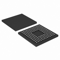
IC ARM7 MCU FLASH 256K 144TFBGA
Manufacturer
NXP Semiconductors
Series
LPC2200r
Datasheet
1.LPC2292FBD144015.pdf
(53 pages)
Specifications of LPC2292FET144/01,5
Core Processor
ARM7
Core Size
16/32-Bit
Speed
60MHz
Connectivity
CAN, EBI/EMI, I²C, Microwire, SPI, SSI, SSP, UART/USART
Peripherals
POR, PWM, WDT
Number Of I /o
112
Program Memory Size
256KB (256K x 8)
Program Memory Type
FLASH
Ram Size
16K x 8
Voltage - Supply (vcc/vdd)
1.65 V ~ 3.6 V
Data Converters
A/D 8x10b
Oscillator Type
Internal
Operating Temperature
-40°C ~ 85°C
Package / Case
144-TFBGA
Processor Series
LPC22
Core
ARM7TDMI-S
Data Bus Width
32 bit
Data Ram Size
16 KB
Interface Type
CAN, I2C, JTAG, SPI, SSP, UART
Maximum Clock Frequency
60 MHz
Number Of Programmable I/os
112
Number Of Timers
2
Operating Supply Voltage
3.3 V
Maximum Operating Temperature
+ 85 C
Mounting Style
SMD/SMT
3rd Party Development Tools
MDK-ARM, RL-ARM, ULINK2
Minimum Operating Temperature
- 40 C
On-chip Adc
10 bit, 8 Channel
Package
144TFBGA
Device Core
ARM7TDMI-S
Family Name
LPC2000
Maximum Speed
60 MHz
For Use With
OM10091 - KIT DEV PHYCORE-ARM7/LPC2220622-1005 - USB IN-CIRCUIT PROG ARM7 LPC2K568-1757 - BOARD EVAL FOR LPC220X ARM MCU
Lead Free Status / RoHS Status
Lead free / RoHS Compliant
Eeprom Size
-
Lead Free Status / Rohs Status
Details
Other names
568-4320
935284897551
LPC2292FET144/01-S
LPC2292FET144/01-S
935284897551
LPC2292FET144/01-S
LPC2292FET144/01-S
Available stocks
Company
Part Number
Manufacturer
Quantity
Price
Company:

Part Number:
LPC2292FET144/01,5
Manufacturer:
NXP Semiconductors
Quantity:
10 000


NXP Semiconductors
LPC2292_2294_7
Product data sheet
6.14.1 Features
6.15.1 Features
6.14 SSP controller (LPC2292/94/01 only)
6.15 General purpose timers
The SSP is a controller capable of operation on a SPI, 4-wire SSI, or Microwire bus. It can
interact with multiple masters and slaves on the bus. Only a single master and a single
slave can communicate on the bus during a given data transfer. Data transfers are in
principle full duplex, with frames of four to 16 bits of data flowing from the master to the
slave and from the slave to the master.
While the SSP and SPI1 peripherals share the same physical pins, it is not possible to
have both of these two peripherals active at the same time. Application can switch on the
fly from SPI1 to SSP and back.
The Timer/Counter is designed to count cycles of the peripheral clock (PCLK) or an
externally supplied clock and optionally generate interrupts or perform other actions at
specified timer values, based on four match registers. It also includes four capture inputs
to trap the timer value when an input signal transitions, optionally generating an interrupt.
Multiple pins can be selected to perform a single capture or match function, providing an
application with ‘or’ and ‘and’, as well as ‘broadcast’ functions among them.
•
•
•
•
•
•
•
•
•
•
Compatible with Motorola’s SPI, Texas Instrument’s 4-wire SSI, and National
Semiconductor’s Microwire buses.
Synchronous serial communication.
Master or slave operation.
8-frame FIFOs for both transmit and receive.
Four to 16 bits per frame.
A 32-bit Timer/Counter with a programmable 32-bit Prescaler.
Timer or external event counter operation
Four 32-bit capture channels per timer that can take a snapshot of the timer value
when an input signal transitions. A capture event may also optionally generate an
interrupt.
Four 32-bit match registers that allow:
– Continuous operation with optional interrupt generation on match.
– Stop timer on match with optional interrupt generation.
– Reset timer on match with optional interrupt generation.
Four external outputs per timer corresponding to match registers, with the following
capabilities:
– Set LOW on match.
– Set HIGH on match.
– Toggle on match.
– Do nothing on match.
Rev. 7 — 4 December 2008
16/32-bit ARM microcontrollers with external memory interface
LPC2292/LPC2294
© NXP B.V. 2008. All rights reserved.
22 of 53
Related parts for LPC2292FET144/01,5
Image
Part Number
Description
Manufacturer
Datasheet
Request
R

Part Number:
Description:
NXP Semiconductors designed the LPC2420/2460 microcontroller around a 16-bit/32-bitARM7TDMI-S CPU core with real-time debug interfaces that include both JTAG andembedded trace
Manufacturer:
NXP Semiconductors
Datasheet:

Part Number:
Description:
NXP Semiconductors designed the LPC2458 microcontroller around a 16-bit/32-bitARM7TDMI-S CPU core with real-time debug interfaces that include both JTAG andembedded trace
Manufacturer:
NXP Semiconductors
Datasheet:
Part Number:
Description:
NXP Semiconductors designed the LPC2468 microcontroller around a 16-bit/32-bitARM7TDMI-S CPU core with real-time debug interfaces that include both JTAG andembedded trace
Manufacturer:
NXP Semiconductors
Datasheet:
Part Number:
Description:
NXP Semiconductors designed the LPC2470 microcontroller, powered by theARM7TDMI-S core, to be a highly integrated microcontroller for a wide range ofapplications that require advanced communications and high quality graphic displays
Manufacturer:
NXP Semiconductors
Datasheet:
Part Number:
Description:
NXP Semiconductors designed the LPC2478 microcontroller, powered by theARM7TDMI-S core, to be a highly integrated microcontroller for a wide range ofapplications that require advanced communications and high quality graphic displays
Manufacturer:
NXP Semiconductors
Datasheet:
Part Number:
Description:
The Philips Semiconductors XA (eXtended Architecture) family of 16-bit single-chip microcontrollers is powerful enough to easily handle the requirements of high performance embedded applications, yet inexpensive enough to compete in the market for hi
Manufacturer:
NXP Semiconductors
Datasheet:
Part Number:
Description:
The XA-S3 device is a member of Philips Semiconductors? XA(eXtended Architecture) family of high performance 16-bitsingle-chip microcontrollers
Manufacturer:
NXP Semiconductors
Datasheet:

Part Number:
Description:
The NXP BlueStreak LH75401/LH75411 family consists of two low-cost 16/32-bit System-on-Chip (SoC) devices
Manufacturer:
NXP Semiconductors
Datasheet:
Part Number:
Description:
The NXP LPC3130/3131 combine an 180 MHz ARM926EJ-S CPU core, high-speed USB2
Manufacturer:
NXP Semiconductors
Datasheet:
Part Number:
Description:
The NXP LPC3141 combine a 270 MHz ARM926EJ-S CPU core, High-speed USB 2
Manufacturer:
NXP Semiconductors
Part Number:
Description:
The NXP LPC3143 combine a 270 MHz ARM926EJ-S CPU core, High-speed USB 2
Manufacturer:
NXP Semiconductors

Part Number:
Description:
The NXP LPC3152 combines an 180 MHz ARM926EJ-S CPU core, High-speed USB 2
Manufacturer:
NXP Semiconductors
Part Number:
Description:
The NXP LPC3154 combines an 180 MHz ARM926EJ-S CPU core, High-speed USB 2
Manufacturer:
NXP Semiconductors

Part Number:
Description:
Standard level N-channel enhancement mode Field-Effect Transistor (FET) in a plastic package using NXP High-Performance Automotive (HPA) TrenchMOS technology
Manufacturer:
NXP Semiconductors
Datasheet: